To extract top performance from a computer system, it is important to understand the architecture of the system.This section describes the architecture of SGI SN0 systems: the Origin 2000, Onyx2, and Origin 200 systems and the components they contain, including the MIPS R10000, R12000, or R14000 CPUs.
The architecture of SN0 (Scalable Node 0) systems form the basis for a scalable multiprocessor with shared memory. The Origin 2000 and Onyx2, as well as the Origin 200, are based on the SN0 architecture. This section describes what a scalable, shared memory multiprocessor is, and explains the rationale for the SN0 architecture.
Because there is always a limit to the performance of a single CPU, computer manufacturers have increased the performance of their systems by incorporating multiple CPUs. Two approaches for utilizing multiple CPUs have emerged: distributed memory, in which each CPU has a private memory; and shared memory, in which all CPUs access common memory.
Previous shared memory computer designs—including the Challenge and Power Challenge systems from SGI —were implemented using a bus architecture: processor boards and memory boards plugged into a single common bus, with all communication between the hardware components occurring over the bus.
A shared-memory architecture has many desirable properties. Each CPU has direct and equal access to all the memory in the system. It is relatively easy to build a single operating system that uses all CPUs in a symmetrical way. Parallel programs are easy to implement on such a system. Parallelism can be achieved by inserting directives into the code to distribute the iterations of a loop among the CPUs. A Fortran loop of this type is shown in Example 1-1.
Example 1-1. Parallel Code Using Directives for Simple Scheduling
subroutine mm11(n,a,lda,r,ldr,s,lds)
      integer n, lda, ldr, lds, i, j, k
      real*8 a(lda,n), r(ldr,n), s(lds,n)
!$OMP PARALLEL DO private(j,k,i), shared(n,a,r,s), schedule(static)
      do j = 1, n
         do k = 1, n
            do i = 1, n
               a(i,j) = a(i,j) + r(i,k)*s(k,j)
            enddo
         enddo
      enddo
      return
      end
|
In Example 1-1, schedule(static) means that blocks of consecutive iterations are assigned to each CPU. That is, if there are p CPUs, the first CPU is responsible for executing the first ceil(n/p) iterations, the second CPU executes the next ceil(n/p) iterations, and so on.
One advantage of this parallelization style is that it can be done incrementally. That is, the user can identify the most time-consuming loop in the program and parallelize just that. (Loops without directives run sequentially, as usual.) The program can then be tested to validate correctness and measure performance. If a sufficient speedup has been achieved, the parallelization is complete. If not, additional loops can be parallelized one at a time.
Another advantage of the shared memory parallelization is that loops can be parallelized without being concerned about which CPUs have accessed data elements in other loops. In the parallelized loop above, the first CPU is responsible for updating the first ceil(n/p) columns of the array a.
In the loop in Example 1-2, a dynamic schedule is used, which means that the first CPU will access every pth column of array a.
Example 1-2. Parallel Code Using Directives for Dynamic Scheduling
subroutine exam12(n,a,lda,b)
      integer n, lda, kb, k
      real*8 a(lda,n), b(n), t
!$OMP PARALLEL DO private(kb,k,t), shared(n,a,b), schedule(dynamic)
      do kb = 1, n
         k = n + 1 - kb
         b(k) = b(k)/a(k,k)
         t = -b(k)
         call daxpy(k-1,t,a(1,k),1,b(1),1)
      enddo
      return
      end
|
Because all memory is equally accessible to all CPUs, nothing special needs to be done for a CPU to access data that were last touched by another CPU; each CPU simply references the data it requires. This makes parallelization easier; the programmer needs only make sure the CPUs have an equal amount of work to do; it doesn't matter which subset of the data is assigned to a particular CPU.
A different approach to multiprocessing is to build a system from many units each containing a CPU and memory. In a distributed memory architecture, there is no common bus to which memory attaches. Each CPU has its own local memory that can only be accessed directly by that CPU. For a CPU to have access to data in the local memory of another CPU, a copy of the desired data elements must be sent from one CPU to the other.
When such a distributed architecture is exposed through the software, the programmer has to specify the exchange of data. Programmed copying of data between CPUs is called message-passing. It is accomplished using a software library. MPI and PVM are two libraries that are often used to write message-passing programs.
To run a program on a message-passing machine, the programmer must decide how the data should be distributed among the local memories. Data structures that are to be operated on in parallel must be distributed. In this situation, incremental parallelism is not possible. The key loops in a program will typically reference many data structures; each structure must be distributed in order to run that loop in parallel. Once a data structure has been distributed, every section of code that references it must be run in parallel. The result is an all-or-nothing approach to parallelism on distributed memory machines. In addition, often a data structure is bigger than a single local memory, and it may not be possible to run the program on the machine without first parallelizing it.
In the preceding section you saw that different loops of a program may be parallelized in different ways to ensure an even allocation of work among the CPUs. To make a comparable change on a distributed memory machine, data structures have to be distributed differently in different sections of the program. Redistributing the data structures is the responsibility of the programmer, who must find efficient ways to accomplish the needed data shuffling. Such issues never arise in the shared memory implementation.
Why would anyone build anything but a shared memory computer? The reason is scalability. Table 1-1 shows the performance of the NAS parallel benchmark kernel running on a Power Challenge 10000 system. Results are presented for a range of CPU counts and for two problem sizes: Class A represents a small problem size, and the Class B problem is four times larger. The columns headed “Amdahl” show the theoretical speedup predicted by Amdahl's law (see “Understanding Parallel Speedup and Amdahl's Law” in Chapter 8).
Table 1-1. Scaling of NAS Parallel Benchmark on a Bus Architecture
#CPUs | Class A (seconds) | Speedup | Amdahl | Class B (seconds) | Speedup | Amdahl |
|---|---|---|---|---|---|---|
1 | 62.73 | 1.00 | 1.00 | 877.74 | 1.00 | 1.00 |
2 | 32.25 | 1.95 | 1.95 | 442.66 | 1.98 | 1.98 |
4 | 16.79 | 3.74 | 3.69 | 225.10 | 3.90 | 3.90 |
8 | 9.58 | 6.55 | 6.68 | 125.71 | 6.98 | 7.54 |
12 | 7.96 | 7.88 | 9.16 | 103.44 | 8.49 | 10.96 |
16 | 7.55 | 8.31 | 11.24 | 98.92 | 8.87 | 14.16 |
Table 1-1 shows that the performance scales well with number of CPUs, through eight CPUs. Then it levels off; the 12-CPU performance is well short of 150% of the 8-CPU performance, and the 16-CPU times are only slightly improved. The cause is the common bus in the shared memory system. It has a finite bandwidth and hence a finite number of transactions that it can transport per second. For this particular program, the limit is reached when 12 CPUs are accessing memory simultaneously. The bus is said to be “saturated” with memory accesses; and when 16 CPUs run the program, the execution time remains almost the same. For other programs, the number of CPUs needed to saturate the bus varies. But once this limit has been reached, adding more CPUs will not significantly increase the program's performance—the system lacks scalability past that limit.
Although a shared memory architecture offers programming simplicity, the finite bandwidth of a common bus can limit scalability. A distributed memory, message-passing architecture cures the scalability problem by eliminating the bus, but it also eliminates the programming simplicity of the shared memory model. The SN0 scalable shared memory architecture aims to deliver the best of both approaches.
In the SN0 design, memory is physically distributed; there is no common bus that could become a bottleneck. Memory is added with each CPU and memory bandwidth grows as CPUs and memory are added to the system. Nevertheless, SN0 hardware presents all memory to software within a unified, global address space. As far as software is concerned, all memory is shared, just as in a bus-based system. The programming ease is preserved, but the performance is scalable.
The improvement in scalability is easily observed in practice. Table 1-2 shows the performance of the NAS parallel benchmark (FT kernel) on an Origin 2000 system.
Table 1-2. Scaling of NAS Parallel Benchmark on the Origin 2000
#CPUs | Class A (seconds) | SpeedUp | Class B (seconds) | Speedup |
|---|---|---|---|---|
1 | 55.43 | 1.00 | 810.41 | 1.00 |
2 | 29.53 | 1.88 | 419.72 | 1.93 |
4 | 15.56 | 3.56 | 215.95 | 3.75 |
8 | 8.05 | 6.89 | 108.42 | 7.47 |
16 | 4.55 | 12.18 | 54.88 | 14.77 |
32 | 3.16 | 17.54 | 28.66 | 28.28 |
You can see that programs with sufficient parallelism now scale to as many CPUs as are available. What's more, this is achieved with the same code that was used on the bus-based shared memory system.
In addition, the per-CPU performance on Origin 2000 systems is better than on Power Challenge 10000 systems (compare the first four rows of Table 1-2 with Table 1-1) because of the improved memory access times of the SN0 system.
To understand scalability in the SN0 architecture, first look at how the building blocks of an SN0 system are connected.
Figure 1-1 shows high-level block diagrams of SN0 systems with various numbers of CPUs. Each “N” square represents a node board, containing CPUs and some amount of memory. Each “R” circle represents a router, a board that routes data between nodes. The dotted lines shown in the 16- and 32-processor systems depict the router connections.
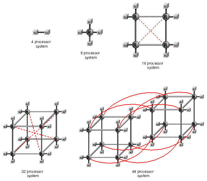
Each SN0 node contains one or two CPUs, some memory, and a custom circuit called the hub. Additionally, I/O can be connected to a node through one or more XIO boards. The hub in a node directs the flow of data between CPUs, memory, and I/O. Through the hub, memory in a node can be used concurrently by one or both CPUs, by I/O attached to the node, and—via a router—by the hubs in other nodes.
The smallest SN0 systems consist of a single node. For example, an Origin 200 system is a deskside unit containing a single node, with one or two CPUs, memory, and I/O.
Larger SN0 systems are built by connecting multiple nodes. The first diagram in Figure 1-1 shows a two-node system, such as an Onyx2 Deskside system. Connecting two nodes means connecting their hub chips. In a two-node system this requires only wiring the two hubs together. The hub on either node can access its local memory, and can also access memory in the other node, through the other hub.
A hub determines whether a memory request is local or remote based on the physical address of the data. (The node number is encoded in the high-order bits of the 64-bit physical address.) Access to memory on a different node takes more time than access to memory on the local node, because the request must be processed through two hubs.
When there are more than two nodes in a system, their hubs cannot simply be wired together. The hardware in an SN0 system that connects nodes is called a router. A router can be connected to up to six hubs or other routers. In the 8-CPU system shown in Figure 1-1, a single router connects four hubs. The router, like a hub, introduces a tiny delay in data transfer, so a CPU in one node incurs an extra delay in accessing memory on a different node.
Now compare the 16-, 32- and 64-CPU system diagrams. From these diagrams you can begin to see how the router configurations scale: each router is connected to two hubs, routers are then connected to each other forming a binary n-cube, or hypercube, in which n, the dimensionality of the router configuration, is the base-2 logarithm of the number of routers.
Because each router can connect to as many as six hubs or other routers, each router also can be connected in a diagonal manner in addition to each 'nearest' neighbor in the 16-processor 'square' or 32-processor 'cube'. For clarity in visualization, these diagonal connections are shown as dashed lines on the diagrams in Figure 1-1. All connections between routers are of equal speed. Memory accesses that involve a path through more than two routers will be slower than for just two routers.
The key point is that the SN0 hardware allows the memory to be physically distributed and yet shared by all software, just as in a bus-based system. Each node contains some local memory (usually many megabytes) that is accessed in the least time. The hardware makes all memory equally accessible from a software standpoint, by routing memory requests through routers to the other nodes. However, the hypercube topology ensures that these data paths do not grow linearly with the number of CPUs: as more nodes and routers are added, more parallel data paths are created. Thus a system can be scaled up without fear that the router connections will become a bottleneck, the way the bus becomes a bottleneck in a bus architecture.
One nice characteristic of the bus-based shared memory systems has been sacrificed: the access time to memory is no longer uniform, but varies depending on how far away the memory lies from the CPU. The two CPUs in each node have quick access through their hub to their local memory. Accessing remote memory through an additional hub adds an extra increment of time, as does each router the data must travel through. This is called nonuniform memory access (NUMA). However, several factors combine to smooth out access times:
The hardware has been designed so that the incremental costs to access remote memory are not large. The choice of a hypercube router configuration means that the number of routers information must pass through is at most n+1, where n is the dimension of the hypercube; this grows only as the logarithm of the number of routers.
As a result, the average memory access time on even the largest SN0 system is no greater than the uniform memory access time on a Power Challenge 10000 system.
The R10000 CPUs operate on data that are resident in their caches. When programs use the caches effectively, the access time to memory (local or remote) is unimportant because the great majority of accesses are satisfied from the caches.
The R10000 CPUs can prefetch data that are not in cache. Other work can be carried out while these data move from local or remote memory into the cache, thus hiding the access time.
Through operating system support or explicit programming, the data of most programs can be made to reside primarily in memory that is local to the CPUs that execute the code.
The SN0 architecture provides shared memory hardware without the limitations of traditional bus-based designs. The following topics look in detail at the components that make up the system.
An Origin 2000 or Onyx2 system starts with a node board. Figure 1-2 displays a block diagram of a node board and the actual appearance of one.
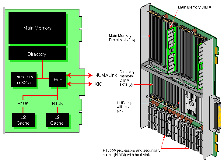
Each node contains two R10000 family CPUs. (An overview of the R10000 CPU appears later; see “Understanding MIPS R10000 Architecture”.) Node boards are available with CPUs that run at different clock rates, from 180 MHz up to 500 MHz, and using different sizes of secondary cache. (The hinv command lists these details for a given system; see the hinv(1) man page.) All the nodes in a system must run at the same clock rate.
In addition to CPUs, a node board has sockets to hold memory DIMMs. A node board can be configured with 64 MB to 4 GB of memory.
In addition to data memory, each main memory DIMM contains extra memory bits. Some of these are used to provide single-bit error correction and dual-bit error detection. The remaining bits store what is known as the cache directory. (The operation of this directory-based cache is described in more detail in a following section; see “Understanding Cache Coherency”.) The use of the cache directory means that the main memory DIMMs must store additional information proportional to the number of nodes in the system. In systems with 32 or fewer CPUs, the directory overhead amounts to less than 6 percent of the storage on a DIMM; for larger systems, it is less than 15 percent. This is comparable to the overhead required for the error correction bits.
SN0 systems can scale to a large number of nodes, and a significant amount of directory information could be required to accommodate the largest configuration. In order not to burden smaller systems with unneeded directory memory, the main memory DIMMs contain only enough directory storage for systems with up to 16 nodes (i.e., 32 CPUs). For larger systems, additional directory memory is installed in separate directory DIMMs. Sockets for these DIMMS are provided below the main memory DIMMs, as can be seen in Figure 1-2.
The final component of the node board is the hub. As described in “Understanding Scalable Shared Memory”, the hub controls data traffic between the CPUs, memory and I/O. The hub has a direct connection to the main memory on its node board. This connection provides a raw memory bandwidth of 780 MBps to be shared by the two CPUs on the node board. In practice, data cannot be transferred on every bus cycle, so the achievable bandwidth is more like 600 MBps.
Access to memory on other nodes is through a separate connection called the NUMAlink interconnect, which attaches to either a router or another hub. The NUMAlink network is bidirectional, and has a raw bandwidth of 780 MBps in each direction. The effective bandwidth achieved is about 600 MBps in each direction, because not all information sent between nodes is user data. To request a copy of a cache line from a remote memory, a hub must first send a 16-byte address packet to the hub that manages the remote memory; this specifies which cache line is desired and where it needs to be sent. Then, when the data are returned, along with the 128-byte cache line of user data, another 16-byte address header is sent (so the receiving hub can distinguish this cache line from others it may have requested). Thus, 16 + 128 + 16 = 160 bytes of data are passed through the NUMAlink interconnect to transfer the 128-byte cache line—so the effective bandwidth is 780 × (128 ÷ 160) = 624 MBps in each direction.
The hub also controls access to I/O devices through a channel called XIO. This connection has the same bandwidth as the NUMAlink connection, but different protocols are used in communicating data. The connection to multiple I/O devices using XIO is described later, under “SN0 Input/Output”.
Each CPU in an SN0 system has a secondary cache memory of 1 MB, 4 MB, or 8 MB. The CPU only fetches and stores data in its cache. When the CPU must refer to memory that is not present in the cache, there is a delay while a copy of the data is fetched from memory into the cache. More details on CPU use of cache memory, and its importance to good performance, is covered in “Cache Architecture”.
The point here is that there could be as many independent copies of one memory location as there are CPUs in the system. If every CPU refers to the same memory address, every CPU's cache will receive a copy of that address. (This can occur when running a parallelized loop that refers to a global variable, for example. It is often the case with some kernel data structures.)
So long as all CPUs only examine the data, all is well; each can use its cached copy. But what if one CPU then modifies that data by storing a new value in it? All the other cached copies of the location instantly become invalid. The other CPUs must be prevented from using what is now “stale data.” This is the issue of cache coherence: how to ensure that all caches reflect only the true state of memory.
Cache coherence is not the responsibility of software (except for kernel device drivers, which must take explicit steps to keep I/O buffers coherent). For performance to be acceptable, cache coherence must be managed in hardware. Furthermore, the cache coherence hardware is external to the R10000 CPU. (The CPU specifies only what the cache must do, not how it does it. The R10000 is used with several different kinds of secondary cache in different systems.)
In the SN0 architecture, cache coherence is the responsibility of the hub chip.
The cache coherence solution in SN0 is fundamentally different from that used in the earlier systems. Because they use a central bus, Challenge and Onyx systems can use a snoopy cache—one in which each CPU board observes every memory access that moves on the bus. When a CPU observes another CPU modifying memory, the first CPU can automatically invalidate and discard its now-stale copy of the changed data.
The SN0 architecture has no central bus, and there is no efficient way for a CPU in one node to know when a CPU in a different node modifies memory on its node or memory in yet a third node. Any scheme that would broadcast memory accesses to every node would cause coherency information to grow as the square of the number of nodes, defeating scalability.
Instead, SN0 uses a different scheme based on a cache directory, which permits cache coherence overhead to scale slowly. (For a theoretical discussion of directory-based caches, see the book by Lenoski and Weber listed under “Third-Party Resources” in the front matter of this book.)
Briefly, here's how directory-based coherency works. As suggested by the diagram in Figure 1-3, the memory in any node is organized as an array of cache lines of 128 bytes. Along with the data bits for each cache line is an extra set of bits, one bit per node. (In large systems, those with more than 128 CPUs, a directory bit represents more than one node, but the principle is the same.) In addition, each directory line contains one small integer, the number of a node that owns that cache line of data exclusively.
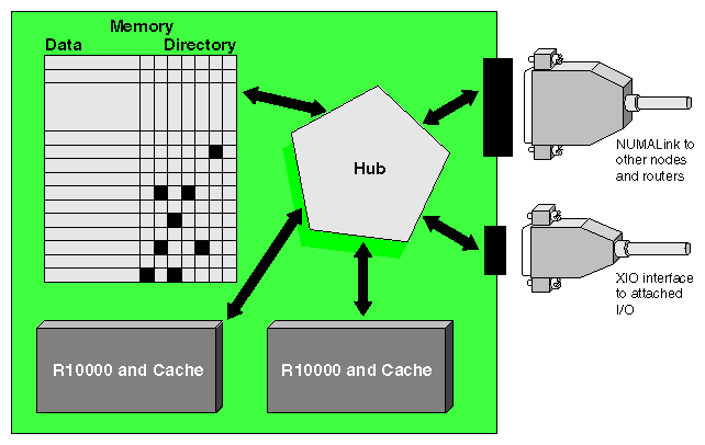
Whenever the hub receives a request for a cache line of data— the request can come from a CPU on the same node, from an attached I/O device, or from some other node via the NUMAlink—the hub checks that line's directory to make sure it is not owned exclusively. Normally it is not, and the hub fetches the whole, 128-byte line and sends it to the requestor.
At the same time, the hub sets “on” the directory bit that corresponds to the requesting node. The requesting node is the current node, if the request came from a CPU or I/O device. When the request comes over the NUMAlink, the requesting node is some other node in the system.
For any line of memory, as many bits can be set as there are nodes in the system. Directory bits are set in parallel with the act of fetching memory; there is no time penalty for maintaining the directory. As long as all nodes that use a cache line only read it, all nodes operate in parallel with no delays.
When a CPU modifies a cache line, it must first gain exclusive ownership. The CPU sends an ownership request to the hub that manages that memory. Whenever the hub receives an ownership request—whether the request comes from a CPU on the same node, or from some other node via the NUMAlink—the hub examines the directory bits of that cache line. It sends an invalidation message to each node for which a bit is set—that is, to each node that has made a copy of the line. Only when this has been done does the hub set the number of the updating node in the directory for that line as the exclusive owner. Then it responds to the requesting node, and that CPU can complete its store operation.
When a hub receives an invalidation message, it removes that cache line from the cache of either (or both) CPUs on its node. In the event those CPUs attempt to refer to that cache line again, they will have to request a new copy, rather than work on the old data.
Typically, invalidations need to be sent to only a small number of other nodes; thus the coherency traffic only grows proportionally to the number of nodes, and there is sufficient bandwidth to allow the system to scale.
When a CPU no longer needs a cache line (for example, when it wants to reuse the cache space for other data), it notifies its hub. The hub sends a release message to the hub that owns the line (if the line is in a different node). If it has exclusive ownership, the hub also sends an updated copy of the cache line. The hub that manages the line removes the exclusive access (if it was set), stores the modified data (if it was modified), and clears the directory bit for the releasing node.
When a CPU wants to read a cache line that is exclusively owned, a more complicated sequence occurs. The request for the line comes to the hub that manages that memory, as usual. That hub observes that some other node has exclusive ownership of the line. Presumably, that owner has modified the data in its cache, so the true, current value of the data is there, not in memory.
The managing hub requests a copy of the line from the owning node. That (owner) hub sends the data to the requesting hub. This retrieves the latest data without waiting for it to be written back to memory.
The SN0 cache coherency design requires other protocols. There is a protocol by which CPUs can exchange exclusive control of a line when both are trying to update it. There are protocols that allow kernel software to invalidate all cached copies of a range of addresses in every node. (The IRIX kernel uses this to invalidate entire pages of virtual memory, so that it can transfer ownership of virtual pages from one node to another.)
The directory-based cache coherency mechanism uses a lot of dedicated circuitry in the hub to ensure that many CPUs can use the same memory, without race conditions, at high bandwidth. As long as memory reads far exceed memory writes (the normal situation), there is no performance cost for maintaining coherence.
However, when two or more CPUs alternately and repeatedly update the same cache line, performance suffers, because every time either CPU refers to that memory, a copy of the cache line must be obtained from the other CPU. This performance problem is generically referred to as cache contention. Two variations of it are:
memory contention, in which two (or more) CPUs try to update the same variables
false sharing, in which the CPUs update distinct variables that only coincidentally occupy the same cache line
Memory contention occurs because of the design of the algorithm; correcting it usually involves an algorithmic change. False sharing is contention that arises by coincidence, not design; it can usually be corrected by modifying data structures.
Part of performance tuning of parallel programs is recognizing cache coherency contention and eliminating it.
As mentioned, the hub controls access to I/O devices as well as memory. Each hub has one XIO port. To allow connections to multiple I/O devices, each hub is connected to a Crossbow (XBOW) I/O controller chip. Up to two hubs may be connected to the same XBOW.
The XBOW is a dynamic crossbar switch that allows up to two hubs to connect to six I/O bus attachments in any combination, as shown in Figure 1-4.
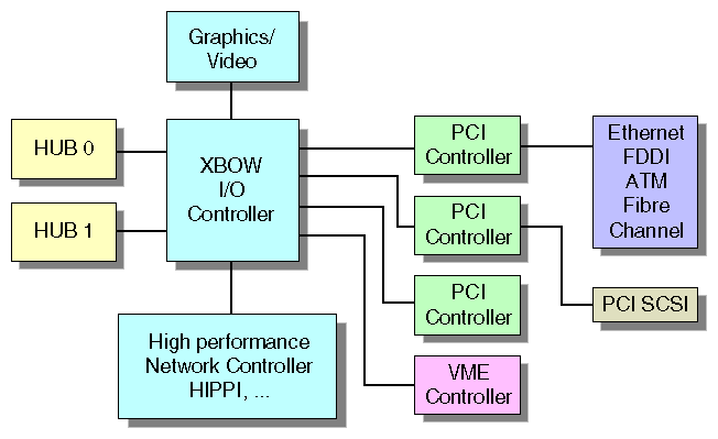
Each XIO connection, from hub to XBOW and from XBOW to I/O device, is bidirectional with a raw bandwidth of 780 MBps in each direction. Like the NUMAlink interconnect, some of the bandwidth is used for control information, so achievable bandwidth is approximately 600 MBps in each direction.
XIO connections to I/O devices are 16 bits wide, although an 8-bit subset may be used for devices for which half the XIO bandwidth is sufficient. Currently, only SGI graphics devices utilize the full 16-bit connection. Industry-standard I/O interfaces such as Ethernet, FDDI, ATM, Fibre Channel, HiPPI, SCSI, and PCI operate at more modest bandwidths, so XIO cards supporting these devices employ the 8-bit subset. Each standard interface card first converts the 8-bit XIO subset to the PCI bus using a custom chip called the PCI adapter. Standard hardware is then employed to convert the PCI bus to the desired interface: VME, Fibrechannel, and so on.
One particular interface card, the IO6, must be installed in every Origin 2000 and Onyx2 system. This I/O card supplies two SCSI buses to provide the minimal I/O requirements of a system; namely, it allows the connection of a CD-ROM drive (for loading system software) and a system disk. It also contains serial and Ethernet ports to allow attachment of a console and external network.
When two nodes are connected to a XBOW, control of the 6 I/O devices is statically partitioned between the two nodes at system boot time. If one node is inoperable, the second can be programmed to take control of all of the devices.
From the standpoint of the XBOW chip, the hub is a portal to and from memory. From the standpoint of the hub, the XBOW is another device that accesses memory, just like a CPU. Software programs the I/O devices to send data from memory out to the device or to read data from the device into memory. In both cases, the device, through the XBOW, requests access to cache lines of memory data.
These requests go to the hub to which the XBOW is attached. If the memory requested is on that node, it is returned. If it is not, the hub passes the request over the NUMAlink interconnect, to get the memory from the node where it resides—exactly as for a CPU's request for memory. In this way, an I/O device attached to any node can read and write to memory anywhere in the system.
We conclude the discussion of the SN0 architecture by summarizing the bandwidths and latencies of different-sized systems. These are shown in Table 1-3.
Table 1-3. Bisection Bandwidth and Memory Latency
Configuration | Bisection Bandwidth |
| Router Hops |
| Read Latency |
|
|---|---|---|---|---|---|---|
Nodes (CPUs) | System (MBps) | Per CPU (MBps) | Maximum | Average | Max (nsec) | Average (nsec) |
1 (2) | n.a. | n.a. | 0 | 0 | 313 | 313 |
2 (4) | 620 | 310 | 0 | 0 | 497 | 405 |
4 (8) | 620 | 310 | 1 | .75 | 601 | 528 |
8 (16) | 620 | 310 | 2 | 1.63 | 703 | 641 |
16 (32) | 620 | 310 | 3 | 2.19 | 805 | 710 |
32 (64) | 310 | 160 | 5 | 2.97 | 1010 | 796 |
64 (128) | 310 | 160 | 6 | 3.98 | 1112 | 903 |
The meanings of the columns of Table 1-3 are as follows:
The number of nodes and CPUs in the system. Larger SN0 systems can be configured in a variety of ways; this table assumes that the optimum arrangement of nodes and routers has been used.
The bisection bandwidth is the total amount of data that can flow in the system concurrently, in megabytes per second of user data. The term “bisection” comes from imagining that the system is bisected by a plane, and measuring the data that crosses that plane.
Bisection bandwidth per CPU is the portion of the total bandwidth that one CPU could use in principle.
Router hops is the number of routers that could handle a request for memory data. The maximum column shows the longest path; the average column is the average over all node-to-node paths. For example, in an 8-CPU system (which uses a single router), each node can access its own memory with zero router hops, but it takes one router hop to get to any of the three remote memories. The average number of hops is thus 0.75.
Read latency is the time to access the first word of a cache line read from memory, in nanoseconds. For local memory, the latency is 313 nanoseconds. For a hub-to-hub direct connection (that is, a two-node configuration), the maximum latency is 497 nsec. For larger configurations, the maximum latency grows approximately 100 nsec for each router hop.
Average latency is calculated by averaging the latencies to all local and remote memories. Even for the 128 CPUs configuration, the average latency is no worse than that of a Power Challenge system, demonstrating that shared memory can be made scalable without negatively affecting performance.
This section describes the features of the MIPS R10000 family of CPUs that are important for performance tuning.
The MIPS R10000, designed to solve many of the performance bottlenecks common to earlier microprocessors, is the CPU used in SN0 systems. SN0 systems have shipped with CPUs running at various clock rates from 195 MHz to 235 MHz.
The R10000 is a four-way superscalar RISC CPU. “Four-way” means that it can fetch and decode four instructions per clock cycle. “Superscalar” means that it has enough independent, pipelined execution units that it can complete more than one instruction per clock cycle. The R10000 contains:
A nonblocking load-store unit that manages memory access.
Two 64-bit integer Arithmetic/Logic Units (ALUs) for address computation and for arithmetic and logical operations on integers.
A pipelined floating point adder for 32- and 64-bit operands.
A pipelined floating point multiplier for 32- and 64-bit operands.
The two integer ALUs are not identical. Although both perform add, subtract, and logical operations, one can handle shifts and conditional branch and conditional move instructions, while the other can execute integer multiplies and divides. Similarly, instructions are partitioned between the floating point units. The floating-point adder is responsible for add, subtract, absolute value, negate, round, truncate, ceiling, floor, conversions, and compare operations. The floating-point multiplier carries out multiplication, division, reciprocal, square root, reciprocal square root, and conditional move instructions.
The two floating-point units can be chained together to perform multiply-then-add and multiply-then-subtract operations, which are single instruction codes. These combined operations, often referred to by their operation codes of madd and msub, are designed to speed the execution of code that evaluates polynomials.
The R10000 can complete most single instructions in one or two clock cycles. However, integer multiple and divide, and floating-point divide and square-root instructions, can occupy one of the ALUs for 20 to 35 clock cycles. Because a number of instructions are in the CPU, being decoded and executed in parallel, the R10000 routinely averages more than one completed instruction per clock cycle, and can reach as many as two instructions per clock cycle in some highly tuned loops.
The R10000 implements the MIPS IV instruction set architecture (ISA). This is the same ISA supported by the MIPS R8000, the CPU used in the Silicon Graphics Power Challenge series, so programs compiled for the older systems are binary-compatible with newer ones. The MIPS IV ISA is a superset of the previous MIPS I, II, and III ISAs that were used in several preceding generations of Silicon Graphics workstations and servers, so programs compiled for those systems are also binary-compatible with the R10000.
The MIPS IV ISA augmented the previous instruction sets with:
Floating point multiply-add (madd and msub) instructions, and reciprocal and reciprocal square root instructions
Indexed loads and stores, which allow coding more efficient loops
Prefetch instructions, which allow the program to request fetching of a cache line in advance of its use, so memory-fetch can be overlapped with execution
Conditional move instructions, which can replace branches inside loops, thus allowing superscalar code to be generated for those loops
This book assumes your programs are written in a high-level language, so you will not be coding machine language yourself. However, the C and Fortran compilers, when told to use the MIPS IV ISA, do take advantage of all these instructions to generate faster code. For this reason it can be worthwhile to recompile an older program.
For more details on the MIPS IV ISA, see the mips_ext(5) man page, and the MIPS R10000 Microprocessor User Guide listed under “Related Manuals”.
The R10000 uses a two-level cache hierarchy: a level-1 (L1) cache internal to the CPU chip, and a level-2 (L2) cache external to it. Both L1 and L2 data caches are nonblocking. That is, the CPU does not stall on a cache miss—it suspends the instruction and works on other instructions. As many as four outstanding cache misses from the combined two levels of cache are supported.
A 32 KB, two-way set associative, instruction cache, managed as an array of 512, 64-byte cache lines.
A 32 KB, two-way set associative, two-way interleaved data cache, managed as an array of 1024, 32-byte cache lines.
These two on-chip caches are collectively called the L1 cache. Whenever the CPU needs an instruction, it looks first in the L1 instruction cache; whenever it needs a data operand it looks first in the L1 data cache. When the data is found there, no memory request is made external to the CPU. The ultimate in speed is achieved when the entire working set of a loop fits in the 64 KB L1 cache. Unfortunately, few time-consuming programs fit in so little memory.
The R10000 CPU can keep exact counts of L1 cache hits and misses. You can take a profile of your program to measure its L1 cache behavior.
When the CPU fails to find the appropriate instructions or data in the L1 cache, it looks next in an off-chip cache consisting of chips on the node board. The L2 cache is a two-way set associative, unified (instructions and data) cache, up to 8 MB in current SN0 systems. The R10000 CPU permits the line size of the L2 cache to be either 64 bytes or 128 bytes, but all SN0 systems use 128-byte cache lines. Both the L1 data cache and the L2 unified cache employ a least recently used (LRU) replacement policy for selecting in which set of the cache to place a new cache line.
The L2 cache can be run at various clock rates, ranging from the same as the CPU down to one-third of that frequency. In current SN0 systems it operates at two-thirds of the CPU frequency.
The R10000 CPU is rare among CPU designs in supporting a set associative off-chip cache. To provide a cost-effective implementation, however, only enough chip terminals are provided to check for a cache hit in one set of the secondary cache at a time. To allow for two-way functionality, an 8,192-entry prediction table is used to record which set of a particular cache address was most recently used. This set is checked first to determine whether there is a cache hit. This takes one cycle and is performed concurrently with the transfer of the first half of the set's cache line. The other set is checked on the next cycle while the second half of the cache line for the first set is being transferred. If there is a hit in the first set, no extra cache access time is incurred. If the hit occurs in the second set, its data must be read from the cache and a minimum four-cycle mispredict penalty is incurred. The net effect is that the time to access the L2 cache is variable, although always much faster than main-memory access.
Cache miss latency to the second-level cache—that is, the time that an instruction is blocked waiting for data from the L2 cache—is from 8 to 12 CPU clock cycles, when the data is found in the L2 cache and the way is correctly predicted.
The R10000 CPU can keep exact counts of L2 cache hits and misses. You can take a profile of your program to measure its L2 cache behavior.
The chief constraint on CPU speed is that the speed of memory is so much slower: a superscalar CPU running at 200 MHz can complete more than one instruction in five nanoseconds. Compare this to the memory latencies shown in Table 1-3. Potentially the CPU could spend the majority of its time waiting for memory fetches. The R10000 CPU uses out-of-order execution and speculative execution in conjunction with its nonblocking caches to try to hide this latency.
From the programmer's point of view, instructions must be executed in predictable, sequential order; when the output of an instruction is written into its destination register, it is immediately available for use in subsequent instructions. Pipelined superscalar CPUs, however, execute several instructions concurrently. The result of a particular instruction may not be available for several cycles. Often, the next instruction in program sequence must wait for its operands to become available, while instructions that come later in the sequence are ready to be executed.
The R10000 CPU dynamically executes instructions as their operands become available—out of order if necessary. This out-of-order execution is invisible to the programmer. What might make out-of-order execution dangerously visible is the possibility of an exception, such as a page fault or a divide-by-zero. Suppose some instructions have been completed out of order when another instruction, which nominally preceded them in the program code, causes an exception. The program state would be ambiguous.
The R10000 CPU avoids this danger by making sure that any result that is generated out of order is temporary until all previous instructions have been successfully completed. If an exception is generated by a preceding instruction, the temporary results can be undone and the CPU state returned to what it would have been, had the instructions been executed sequentially. When no exceptions occur, an instruction executed out of order is “graduated” once all previous instructions have completed; then its result is added to the visible state of the CPU.
Up to 32 instructions may be active in the CPU at a given time, enough to hide at least eight cycles of latency. These instructions are tracked in an active list. Instructions are added to the active list when they are decoded and are removed upon graduation.
Queues are used to select which instructions to issue dynamically to the execution units. Three separate 16-entry queues are maintained: an integer queue for ALU instructions, a floating-point queue for FPU instructions, and an address queue for load and store instructions. Instructions are placed on the queues when they are decoded. Integer and floating-point instructions are removed from their respective queues once the instructions have been issued to the appropriate execution unit. Load and store instructions remain in the address queue until they graduate, because these instructions can fail and may need to be reissued; for example, a data cache miss requires the instruction to be reissued.
When the CPU encounters a conditional branch, the input operand of the branch may not be ready, in which case the CPU does not know which instruction should follow the branch. Older pipelined CPUs had no choice but to stall when they encountered a branch, and wait until the branch operand was available before continuing.
The R10000 CPU instead makes a guess: it predicts which way the branch will likely go, and continues executing instructions speculatively along that path. That is, it predicts whether or not the branch will be taken, and fetches and executes subsequent instructions accordingly. If the prediction is correct, execution proceeds without interruption. If the prediction is wrong, however, any instructions executed down the incorrect program path must be canceled, and the CPU must be returned to the state it was in when it encountered the mispredicted branch.
The R10000 may speculate on the direction of branches nested four deep. To predict whether or not to take the branch, a 2-bit algorithm, based on a 512-entry branch history table, is used. Simulations have shown the algorithm to be correct 87% of the time on the SpecInt92 suite.
The R10000 CPU can keep exact counts of branch prediction hits and misses. You can take a profile of your program to measure how many branches it executed and what percentage were mispredicted. For more information, see Chapter 4, “Profiling and Analyzing Program Behavior”.
The SN0 architecture and the MIPS R10000 CPU together make up a very sophisticated computing environment:
At the micro level of a single instruction stream, the CPU queues as many as 32 instructions, executing them out of order as their operands become available from memory, and speculatively predicting the direction that branches will take. It also manages two levels of cache memory.
At the memory level, the system caches memory at multiple levels: the on-chip L1 cache; the off-chip L2 cache of up to 8 MB; the local node's main memory of 64 MB or more (usually much more); and the total memory of every node in the system—up to 63 other nodes, all equally accessible in varying amounts of time.
At the node level, the hub chip directs the flow of multiple, 780 MBpsec, streams of data passing between memory, two L2 caches, an XBOW chip, and a NUMAlink connection that may carry requests to and from 127 other hubs.
At the system level, multiple I/O buses of different protocols—PCI, VME, SCSI, HIPPI, FibreChannel, and others—can stream data through their XBOWs to and from the memory resident in any node on the system; all concurrent with program data flowing from node to node as requested by multiple IRIX processes running in each CPU in each node.
It is a major triumph of software design that all these facilities can be presented to you, the programmer, under a relatively simple programming model: one program in C or Fortran, with multiple, parallel threads executing the same code. The next chapter examines this programming model.