This chapter describes IRIX 6.5 VME support for Origin 2000 and Onyx2 systems. This chapter gives a high-level overview of the VME bus, and describes how the VME bus is attached to an Origin 2000 or Onyx2 system and how it is configured.
| Note: This chapter has no information about VME in Challenge and Onyx systems. For those systems, refer to Chapter 14, “VME Device Attachment on Challenge/Onyx”, and Chapter 15, “Services for VME Drivers on Challenge/Onyx”. |
This chapter contains important details on VME operation if you are writing a kernel-level VME device driver. It contains useful background information if you plan to control a VME device from a user-level program.
“Overview of the VME Bus” summarizes the history and features of the VME bus architecture.
“About VME Bus Attachment” gives a conceptual overview of how VME support is provided in all SGI systems that have it.
“About VME Bus Addresses and System Addresses” describes the important relationship between addresses on the VME bus and addresses in the physical address space of the system.
“About VME in the Origin2000” documents the hardware details of the VME implementation on Origin 2000 and Origin 200 systems.
“Configuring VME Devices” tells how to configure a device so that IRIX 6.4 can recognize it and initialize its device driver.
More information about VME device control appears in these chapters:
Chapter 4, “User-Level Access to Devices”, covers PIO and DMA access from the user process.
Chapter 13, “Services for VME Drivers on Origin 2000/Onyx2”,discusses the kernel services used by a kernel-level VME device driver, and contains an example.
The VME bus was standardized in the early 1980s. It was designed as a flexible interconnection between multiple master and slave devices using a variety of address and data precisions. While VME is not the fastest bus design available, its well-defined protocols, comparatively low signaling speeds, and ample board dimensions make it an easy bus to design for, whether to create intelligent I/O devices or special-purpose and one-off interfaces. As a result, VME has become a popular standard bus used in a variety of general-purpose and embedded products.
In its original applications, the VME bus was used as the primary system bus, with a CPU card as the principal (or only) bus master. In SGI systems, however, the VME bus is treated as an I/O device—it is never the main system bus.
The VME bus descends from the VERSAbus, a bus design published by Motorola, Inc., in 1980 to support the needs of the MC68000 line of microprocessors. The bus timing relationships and some signal names still reflect this heritage, although the VME bus is used by devices from many manufacturers today.
The original VERSAbus design specified a large form factor for pluggable cards. Because of this, it was not popular with European designers. A bus with a smaller form factor but similar functions and electrical specifications was designed for European use, and promoted by Motorola, Phillips, Thompson, and other companies. This was the VersaModule European, or VME, bus. Beginning with rev B of 1982, the bus quickly became an accepted standard. (For ordering information on the standards documents, see “Standards Documents”.)
A VME bus is a set of parallel conductors that interconnect multiple processing devices. The devices can exchange data in units of 8, 16, 32 or 64 bits during a bus cycle.
Each VME device associates itself with a range of bus addresses. A bus address has either 16, 24, 32, or 64 bits of precision. Each width of address forms a separate address space. That is, the same numeric value can refer to one device in the 24-bit address space, and to a different device in the 32-bit address space. Typically, a device operates in only one address space, but some devices can be configured into multiple address spaces.
Each VME bus cycle contains the bits of an address. The address is qualified by sets of address-modifier bits that specify the following:
the address space (A16, A24, A32, or A64)
whether the operation is single or a block transfer
whether the access is to what, in the MC68000 architecture, would be data or code, in a supervisor or user area. SGI systems support only data area transactions, supervisor-data or user-data.
Each VME device acts as either a bus master or a bus slave. Typically a bus master is a programmable device with a microprocessor—for example, a disk controller. A slave device is typically a nonprogrammable device like a memory board or set of A/D inputs.
Each data transfer is initiated by a master device. The master
asserts ownership of the bus
specifies the address modifier bits for the transfer, including the address space, single/block mode, and supervisor/normal mode
specifies the address for the transfer
specifies the data unit size for the transfer (8, 16, 32 or 64 bits)
specifies the direction of the transfer with respect to the master
The VME bus design permits multiple master devices to exist on the bus, and provides a hardware-based arbitration system so that they can share the bus in alternation.
A slave device responds to a master when the master specifies one of the slave's addresses. The addressed slave accepts data, or provides data, as directed.
The VME design allows for four types of data transfer bus cycles:
A read cycle returns data from the slave to the master.
A write cycle sends data from the master to the slave.
A read-modify-write cycle takes data from the slave, and on the following bus cycle sends it back to the same address, possibly altered.
A block-transfer transaction sends multiple data units to adjacent addresses in a burst of consecutive bus cycles.
The VME design also allows for interrupts. A device can raise an interrupt on any of seven interrupt levels. The interrupt is acknowledged by a bus master. The bus master interrogates the interrupting device in an interrupt-acknowledge bus cycle, and the device returns an interrupt vector number.
In SGI systems, VME interrupts are received by the VME controller. If the controller has been configured by a VECTOR statement (see “Entry Point edtinit()” in Chapter 7) to handle a given interrupt level, it acknowledges the interrupt and sends an interrupt to one of the CPUs in the system.
If the controller has not been configured to acknowledge an interrupt level, the interrupt level is ignored and can be handled by another device on the VME bus.
The VME bus was designed as the system backplane for a workstation, supporting one or more CPU modules along with the memory and I/O modules they used. However, no SGI computer uses the VME bus as the system backplane. In all SGI computers, the main system bus that connects CPUs to memory is a proprietary bus design. The VME bus is attached to the system as an I/O device.
This section provides a conceptual overview of the design of the VME bus in any SGI system. It is sufficient background for most users of VME devices. A more detailed look at the hardware follows in later topics
A VME bus controller is attached to the system bus to act as a bridge between the system bus and the VME bus. This arrangement is shown in Figure 12-1.
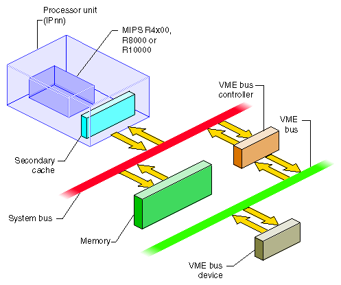
On the SGI system bus, the VME bus controller acts as an I/O device. On the VME bus, the bus controller acts as a VME bus master. The VME controller has several tasks. Its most important task is mapping—that is, translating—some range of physical addresses in the SGI system address space to a range of VME bus addresses. The VME controller performs a variety of other duties for different kinds of VME access.
During programmed I/O (PIO) to the VME bus, software in the CPU loads or stores the contents of CPU registers to a device on the VME bus. The operation of a CPU load from a VME device register is as follows:
The CPU executes a load from a system physical address.
The physical address is placed on a system bus.
The VME controller recognizes the address as one it has been programmed to map.
The VME controller translates the system address to an address in one of the VME bus address spaces.
Acting as a VME bus master, the VME bus controller starts a read cycle on the VME bus, using the translated address.
A device on the VME bus responds to the VME address and returns data.
The VME controller initiates a system bus cycle to return the data packet to the CPU, thus completing the load operation.
A VME device store is similar except it performs a VME bus write; no data is returned.
PIO input and output are fundamentally different in the following way: PIO input requires two system bus cycles—one to request the data and one to return it—separated by the cycle time of the VME bus. PIO output takes only one system bus cycle, and the VME bus write cycle run concurrently with the next system bus cycle. As a result, PIO input always takes at least twice as much time as PIO output.
The MIPS R10000 CPU can execute instructions out of sequence, leaving a memory-load operation pending while executing instructions that logically follow, provided that those instructions do not depend on loaded data. PIO input requires a microsecond or more, a time during which an R10000 can execute 200 or more instructions. An R10000 can execute many instructions following a PIO load before the CPU has to stall and wait for the PIO data to arrive. In a similar way, the R10000 CPU can execute hundreds of instructions after the beginning of a PIO write, concurrently with the output operation.
A VME device that can act as a bus master can perform DMA into system memory. The general sequence of operations in this case is as follows:
The device driver allocates a DMA map object to represent the operation. When the kernel creates the DMA map, it programs the VME controller to map a certain range of VME bus addresses to a range of system memory locations.
The device driver uses PIO to program the device registers of the VME device, instructing it to perform DMA to the assigned range of VME bus address for a specified length of data.
The VME bus master device initiates the first read, write, block-read, or block-write cycle on the VME bus.
The VME controller, recognizing a mapped address, responds as a slave device on the VME bus.
If the bus master is writing, the VME controller accepts the data and initiates a system bus cycle to write the data to system memory at the mapped address.
If the bus master is reading, the VME controller uses a system bus cycle to read data from system memory, and returns the data to the bus master.
The bus master device continues to use the VME controller as a slave device until it has completed the DMA transfer.
During a DMA transaction, the VME bus controller operates independently of any CPU. CPUs in the system execute software concurrently with the data transfer. Since the system bus is faster than the VME bus, the data transfer typically takes place at the maximum data rate that the VME bus master can sustain.
In the Origin2000 and Onyx2 systems (and in the Challenge and Onyx lines), the VME controller contains an additional “DMA Engine” that can be programmed to perform DMA-type transfers between memory and a VME device that is a slave, not a bus master. The general course of operations in a DMA engine transfer is as follows:
The VME bus controller is programmed to perform a DMA transfer to a certain physical memory address for a specified amount of data from a specified device address in VME address space.
The VME bus controller, acting as the VME bus master, initiates a block read or block write to the specified device.
As the slave device responds to successive VME bus cycles, the VME bus controller transfers data to or from memory using the system bus.
The DMA engine transfers data independently of any CPU, and at the maximum rate the VME bus slave can sustain. In addition, the VME controller collects smaller data units into blocks of the full system bus width, minimizing the number of system bus cycles needed to transfer data. For both these reasons, DMA engine transfers are faster than PIO transfers for all but very short transfer lengths. (For details, see “DMA Engine Bandwidth” on page 72.)
Devices on the VME bus exist in one of the following address spaces:
The 16-bit space (A16) permits addresses from 0x0000 to 0xffff.
The 24-bit space (A24) permits addresses from 0x00 0000 to 0xff ffff.
The 32-bit space (A32) permits addresses 0x0000 0000 to 0xffff ffff.
The 64-bit space (A64), defined in the revision D specification, uses 64-bit addresses.
The SGI system bus uses 64-bit numbers to address memory and other I/O devices on the system bus (discussed in Chapter 1, “Physical and Virtual Memory”). Much of the physical address space is used to address system memory. Portions of physical address space are set aside dynamically to represent VME addresses. Parts of the VME address spaces are mapped, that is, translated, into these ranges of physical addresses.
The translation is performed by the VME bus controller: It is programmed to recognize certain ranges of addresses on the system bus and translate them into VME bus addresses; and it recognizes certain VME bus addresses and translates them into physical addresses on the system bus.
The entire A32 or A64 address space cannot be mapped into the physical address space. No SGI system can provide access to all VME address spaces at one time. Only parts of the VME address spaces are available at any time. The limits on how many addresses can be mapped at any time are different in different architectures.
In a user-level program you can perform PIO and certain types of DMA operations (see Chapter 4, “User-Level Access to Devices”). You call on the services of a kernel-level device driver to map a portion of VME address space into the address space of your process. The requested segment of VME space is mapped dynamically to a segment of your user-level address space—a segment that can differ from one run of the program to the next.
In a kernel-level device driver, you request mappings for both PIO and DMA operations using maps—software objects that represent a mapping between kernel virtual memory and a range of VME bus addresses.
| Note: The remainder of this chapter has direct meaning only for kernel-level drivers. |
The addressing needs of PIO access and DMA access are different.
PIO deals in small amounts of data, typically single words. PIO is directed to device registers that are identified with specific VME bus addresses. The association between a device register and its VME address is fixed, typically by setting jumpers or switches on the VME card.
DMA deals with extended segments of kilobytes or megabytes. The addresses used in DMA are not fixed in the device, but are programmed into it just before the data transfer begins. For example, a disk controller can be programmed to read a certain disk sector and write the sector data to a range of 512 consecutive bytes in the VME bus address space. The programming of the disk controller is done by storing numbers into its registers using PIO. While the registers respond only to fixed addresses that are configured into the board, the address for sector data is just a number that is programmed into the controller before a transfer is to start.
These are the key differences between PIO addresses and addresses used for DMA:
PIO addresses are relatively few in number and cover small spans of data, while DMA addresses can span large ranges of data.
PIO addresses are closely related to the hardware architecture of the device and are configured by hardware or firmware, while DMA addresses are simply parameters programmed into the device before each operation.
In systems supported by IRIX 6.4, all mappings from VME address spaces to system physical memory are dynamic, assigned as needed. Kernel functions are provided to create and use map objects that represent the translation between designated VME addresses and kernel addresses (described in detail in Chapter 13, “Services for VME Drivers on Origin 2000/Onyx2”). An Origin2000 system can support a maximum of five VME bus adapters per module. Although a system can comprise numerous modules, there is also a limit of five VME bus adapters, total, per system.
Normally a VME card can be programmed to use different VME addresses for PIO, based on jumper or switch settings on the card. Each device plugged into a single VME bus must be configured to use unique addresses. Errors that are hard to diagnose can arise when multiple cards respond to the same bus address. Devices on different VME buses can of course use the same addresses.
Not all parts of each address space are accessible. The accessible parts are summarized in Table 12-1.
Table 12-1. Accessible VME PIO Addresses on Any Bus
Address Space | Origin2000 Systems | Challenge and Onyx Systems |
|---|---|---|
A16 | All | All |
A24 | 0x80 0000–0xFE 0000 | 0x80 0000–0xFF FFFF |
A32 | 0x0000 0000–0x7FFF FFFF | 0x0000 0000–0x7FFF FFFF |
There are additional limits on the maximum size of any single PIO map and limits on the aggregate size of all maps per bus. These limits differ between the Origin 2000 and the Challenge architectures; the details are given in the discussion of allocating maps.
In general, however, when configuring the devices on a bus, it is best if you can locate all device registers in a single, relatively compact, range of addresses. This economizes on kernel resources used for mapping.
When you program a bus master to perform DMA, you load it with a starting target address in one of the VME address spaces, and a length. This address and length is dynamically mapped to a corresponding range of memory addresses. You can obtain a map to memory for a range of addresses in any of the A16, A24, or A32 data address spaces. The A64 address space is not available for either PIO or DMA on Origin 2000 or Onyx2 systems.
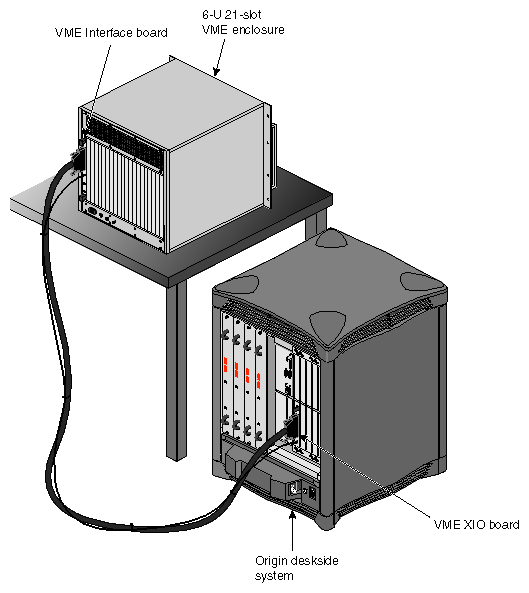
In the Origin 2000 (including Origin Deskside) and Onyx2 systems, external I/O is provided through the XIO interface. The VME bus and adapter is an external I/O device interfaced through one XIO slot. A typical installation is shown in Figure 12-2.
For more information about the external features, options, and availability of the VME Expansion unit, you can consult one of these sources:
Marketing Information | |
Owner's Guide | VME Option Owner's Guide, document number 007-3618-nnn |
The VME controller for Origin 2000 is physically located on a VME board plugged into the VME bus enclosure. It is logically connected to the system as shown in Figure 12-3.
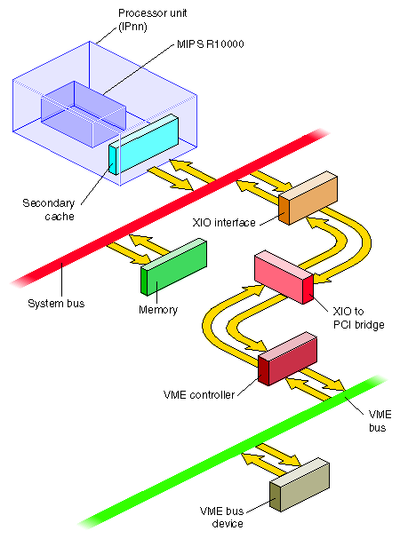
As suggested by Figure 12-3, data to and from the VME bus passes through multiple layers of bus protocols. For example, on a PIO write from the CPU to a VME device, the following functional units are involved:
The CPU sends a word to a physical memory address.
In the Origin 2000 architecture, physical addressing is managed by the Hub chip on the node board (not shown). The Hub chip directs the word to the XIO interface.
The XIO interface passes the word down the Craylink cable (see Figure 12-2) to the VME controller board, which is a VME 6U or 9U card mounted in the card cage.
On the VME controller board, an XIO-to-PCI converter called a Bridge chip. The transaction is converted to a PCI bus write.
The sole device on the PCI bus is the VME controller, a PCI-to-VME bridge chip.
The VME controller operates the signal and data lines of the VME enclosure to execute a write the desired VME address.
The VME controller chip is a PCI-to-VME bridge named the Universe II, produced by Tundra Semiconductor Corporation (http://www.tundra.com ).
The Universe II contains:
FIFO buffers for asynchronous staging of data between the two buses.
Mapping registers for translating VME bus addresses.
A DMA engine comparable to the DMA engine in the Challenge systems, with the added ability to handle linked lists of data (scatter/gather). This engine is accessible only to user-level processes through the udmalib interface.
The ability to pack and unpack multiple D8, D16 and D32 data units from 64-bit PCI data words.
It is important to note that although the data path spans three different bus protocols and multiple bus controller chips, none of these controllers are directly accessible to a VME device driver. The device driver calls on the kernel to create software objects called maps, either PIO maps or DMA maps. When the kernel creates a map, it sets up all the multiple layers of hardware needed to implement that map. The driver uses the map to obtain physical addresses that can be used as if they were wired directly to the VME bus. All the layers of protocol translation between memory and the VME device are transparent to the device driver.
In the event you possess the Tundra Corp Data book describing the Universe II, the settings of important Universe II control registers is listed in Table 12-2. This table is provided for information only. The Universe II registers are loaded by the kernel VME support, and none of these settings is accessible to the device driver. Also, this information is subject to change from release to release.
Table 12-2. Universe II Register Settings
Register | Field | Purpose | Setting |
|---|---|---|---|
MAST_CTL | PWON | Max posted write length | 4096 |
MAST_CTL | VRL | VMEbus Request Level | 3 |
MAST_CTL | VRM | VMEbus Request Mode | demand |
MAST_CTL | VREL | VMEbus Release Mode | On-request |
MAST_CTL | VOWN | VME ownership | n.a. |
MAST_CTL | PABS | PCI Burst Size | 128 bytes |
MISC_CTL | VBTO | Vmebus timeout | 64us |
MISC_CTL | VARB | VMEbus arbitration type | priority |
MISC_CTL | VARBTO | VMEbus arbitration timeout | 16us |
MISC_CTL | RESCIND | VMEbus DTACK* release | rescind |
MISC_CTL | SYSCON | Universe is system controller at power-up | on |
MISC_CTL | V64AUTO | Auto slot ID | n.a. |
You (or the system administrator) must configure a VME bus and device to the IRIX system in order to direct interrupts and to associate each VME device with its device driver. In order to configure the bus you need to know how VME devices are represented in the hardware graph (see “Hardware Graph” in Chapter 2).
Each VME bus is entered into the IRIX hardware graph during bootstrap, as a connection point for devices and as a source of interrupts.
The actual hardware graph path to a VME bus has this form:
/hw/module/mod/slot/ion/baseio/vme_xtown/pci/7/vmebus/ |
The integer mod is the number of the Origin module to which the VME option is attached. Vertex ion designates the XIO slot to which the VME option is cabled.
The hwgraph vertex named vmebus represents the VME controller. Vertexes for devices on the bus are found under that vertex. A convenience path is also created for each bus in the form:
/hw/vme/b/ |
The bus number b is assigned by the ioconfig command (see “Using ioconfig for Global Controller Numbers” in Chapter 2). The number b is arbitrarily assigned the first time ioconfig runs after a VME option is added to the system. The first VME bus must be number 1 (not 0).
The bus numbers as assigned are recorded in the ioconfig database file /etc/ioconfig.config (see “Configuration Control File” in Chapter 2). The administrator can edit that file to change the numbering, for example to force a certain bus to be number 1.
In order to direct VME bus interrupt levels to specified CPUs, you need to be able to name the interrupt levels of a bus. For this purpose, the kernel creates names of the following form in the hwgraph:
/hw/module/mod/slot/ion/baseio/vme_xtown/pci/7/vmebus/ipl/i |
Seven of these names appear under each vmebus vertex, with i ranging from 1 to 7. Each vertex represents one VME bus interrupt priority level.
The same vertexes are accessible under the convenience names:
/hw/vme/b/ipl/i |
You can use either of these pathnames in a DEVICE_ADMIN command to direct VME interrupts.
VME interrupts are handled in two phases. The first phase, which executes at a high priority and is extremely quick, involves acknowledging the interrupt and locating the device driver interrupt handler that should be notified. In the second phase, the device driver's specified handler executes as an independent thread (see “Handling VME Interrupts” in Chapter 13).
The first phase of processing executes on the CPU to which the interrupt is directed by hardware. When nothing is done, all interrupts from a VME bus controller are directed to CPU 0 in the Origin module to which the VME bus is attached.
The system administrator can use the DEVICE_ADMIN statement to direct VME interrupts to a specific CPU. The DEVICE_ADMIN statement is placed in a file in the /var/sysgen/system directory, possibly (but not necessarily) /var/sysgen/system/irix.sm. The form of the statement to direct interrupts is:
DEVICE_ADMIN: device_path INTR_TARGET=cpu_path |
The device_path is the hwgraph path specifying one of the VME interrupt levels for a bus (see “VME Bus and Interrupt Naming”). The cpu_path is the hwgraph path that specifies a CPU. For example, to send VME level-7 interrupts from the first VME bus to CPU 12, you could write
DEVICE_ADMIN: /hw/vme/1/ipl/7 INTR_TARGET=/hw/cpunum/12 |
Although there are seven VME interrupt levels, only six unique redirections of this type can be supported for any VME bus. In other words, you can direct the seven levels to at most six different CPUs. You must send at least two levels to the same CPU. (Typically you direct all the levels to a single CPU.)
The DEVICE_ADMIN statement directs interrupt detection. The device driver itself specifies the CPU in which the interrupt handler code executes. By default this is the same CPU where detection takes place.
VME devices are entered as vertexes in the hwgraph while the VECTOR statements are processed during system startup. The kernel creates a vertex for each device with the following form:
/hw/module/mod/slot/ion/baseio/vme_xtown/pci/7/vmebus/assm/addr/ |
The vertex shown here as assm is the name of the VME address space, one of a16s, a16n, a24s, a24n, a32s, or a32n. The vertex addr is the primary address of the device, from its VECTOR statement. The address is in hexadecimal digits with leading zeros suppressed. For example, a device located at 0x00108000 in the A32 non-supervisory space would appear in the hwgraph as
/hw/module/mod/slot/ion/baseio/vme_xtown/pci/7/vmebus/a32n/108000 |
The same vertex appears also under the convenience vertex for that bus:
/hw/vme/b/a32n/108000 |
This kernel-created vertex is the “connection point” that is passed to the device driver when the driver is called to initialize the device. The device driver is allowed (encouraged) to create additional vertexes with more meaningful names (the initialization process is described under “Initializing a VME Device” in Chapter 13).
Devices on the VME bus do not identify themselves to the system automatically (as devices on the PCI bus do). You must tell IRIX that a device exists, or should exist. You do this using the VECTOR statement. The VECTOR statement is placed in a file in the directory /var/sysgen/system (see “Kernel Configuration Files” in Chapter 2). For VME, the syntax of the VECTOR statement is as follows:
VECTOR: bustype=VME module=modname [ adapter=b [ ctlr=c ] ]
     [ ipl=i ] [ vector=v ]
       iospace=(AnnM,addr,size)
     [ iospace2=(AnnM,addr,size) ]
     [ iospace3=(AnnM,addr,size) ]
     [ exprobe=((cmd,paddr,width,value,mask) [,...] ]
|
The variable elements of this statement, in order of appearance, are as follows:
modname | Name of the configuration file for the device driver for this type of device (see “Master Configuration Database” in Chapter 2 ). |
b | Number of the VME bus as assigned by ioconfig (see “VME Bus and Interrupt Naming” ) |
c | Arbitrary number to distinguish this device to the driver. |
i | Interrupt priority level used by this device, if it produces interrupts. |
v | Interrupt vector value returned by this device, when that is known (some devices are dynamically configured with vector numbers by the driver). |
AnnM | Name of the address space used by this device, one of A16S, A16NP, A24S, A24NP, A32S, A32NP |
addr | Lowest address in a range of addresses used by the device. |
size | Number of bytes in the range of addresses. |
cmd | Probe command, either w meaning write, r meaning read and test equal, or rn meaning read and test not-equal. |
paddr | Address to probe (in the address space given by iospace). |
width | The width of data to read or write in the probe: 1, 2, 4 or 8 bytes. |
value | A value to be written, or to be compared to the data returned by read. |
mask | A mask to be ANDed with the value before writing, or to be ANDed with the data returned by a read before comparison. |
Numeric values (variables b, c, i, v, nn, addr, size, paddr, width, value and mask) can be written in decimal, or in hexadecimal with a prefix of “0x.”
| Note: The VECTOR statement is written as a single physical line in a text file. In this book, VECTOR statements are broken across multiple lines for readability. Do not break a VECTOR statement across multiple text lines in a configuration file. |
As an example, imagine you have two VME boards on bus number 1, with these features:
Reside in A32NP address spaces starting 0x001008000 and 0x00108020 respectively.
Support 8, 4-byte registers.
Writing a zero word into the first register resets a board; after which the least significant bit of the eighth register should be zero.
The driver for this type of board is configured in a file named /var/sysgen/master.d/vme_examp.
Jumpered to generate interrupts on IPL 5 with vectors of 0x0e and 0x0f respectively.
To configure these boards you could prepare a file named /var/sysgen/system/twoboards.sm with these contents:
Example 12-1. Hypothetical VME Configuration File
* First board, "controller" 0, base 10 8000, vector 0e
VECTOR: bustype=VME module=vme_examp adapter=1 ctlr=0
        ipl=5 vector=0x0e iospace=(A32NP,0x00108000,32)
        exprobe=((w,0x001080000,4,0,0),(r,0x0010801c,4,0,1))
* Second board, "controller" 1, base 10 8020, vector 0f
VECTOR: bustype=VME module=vme_examp adapter=1 ctlr=1
        ipl=5 vector=0x0f iospace=(A32NP,0x00108020,32)
        exprobe=((w,0x001080020,4,0,0),(r,0x0010803c,4,0,1))
|
You use the exprobe= parameter to specify one or more PIO writes and reads to the bus. You can use the parameter to initialize multiple registers, and to test the values in multiple registers before or after writing.
The primary purpose of the exprobe parameter is to make the call to a device driver conditional on the presence of the device. When the probe fails because a read did not return the expected value, the kernel assumes the device is not present (or is not operating correctly, or is the wrong type of device), and the kernel does not call the device driver to initialize the device.
When you do not specify a probe sequence, the kernel assumes the device exists, and calls the driver to initialize the device. In this case, the driver can be called when no device is present. You must write code into the driver to verify that a device of expected type is actually present on the bus. (See “Verifying Device Addresses” in Chapter 13.)
VECTOR statements are processed in two sets, depending on whether or not the adapter=b parameter is present. The presence or absence of this parameter has an important effect on the scope and timing of device initialization.
When you omit adapter=b, the kernel applies the VECTOR statement to every VME bus in the system. The exprobe, if one is given, is executed against every VME bus found, as soon as the bus is found. The device driver is called when a probe succeeds on a bus. The driver is called for every bus when no probe is given
When you specify adapter=b, the kernel does not execute the VECTOR statement until after all buses have been found, and ioconfig has run to apply numbering to the buses. Then the kernel executes these VECTOR statements, applying each one only to the bus you specify.
The differences are that, with adapter=b, the probe is executed and the driver called only for the specified bus, and this occurs quite a bit later in the startup sequence. It is almost always a better idea to code adapter=b than to omit it.
Assuming that adapter=b is supplied, the following steps take place:
The kernel discovers each VME bus and builds a hwgraph vertexes for it.
The ioconfig program runs and numbers the buses.
The kernel processes the VECTOR statements.
The kernel executes the specified probes; for example, assuming the first statement in Example 12-1, the kernel writes a word of zero to A32NP address 0x0010080000, then reads a word from address 0x001008001c, ANDs the returned data with 1, and compares the result to 0. If the comparison is equal, the device exists.
When the probe succeeds, the kernel creates hwgraph vertices for the device; given Example 12-1 it might build:
/hw/module/mod/slot/ion/baseio/vme_xtown/pci/7/vmebus/a32n/1008000
/hw/vme/1/a32n/1008000
The kernel loads the specified device driver (if necessary) and calls it to initialize the device, passing it much of the information from the VECTOR statement.