This chapter gives a high-level overview of the VME bus, and describes how the VME bus is attached to, and operated by Challenge and Onyx systems.
| Note: For information on hardware device issues on the Origin 2000 and Onyx2 platforms, refer to Chapter 12, “VME Device Attachment on Origin 2000/Onyx2”, and Chapter 13, “Services for VME Drivers on Origin 2000/Onyx2”.. |
This chapter contains useful background information if you plan to control a VME device from a user-level program. It contains important details on VME addressing if you are writing a kernel-level VME device driver.
“Overview of the VME Bus” summarizes the history and features of the VME bus architecture.
“VME Bus in Challenge and Onyx Systems” gives an overview of how the VME bus is integrated into Challenge and Onyx computer systems.
“VME Bus Addresses and System Addresses” discusses the relationship between addresses on the VME bus and addresses in the physical address space of the system.
“Configuring VME Devices” tells how to configure a device so that IRIX can recognize it and initialize its device driver.
“VME Hardware in Challenge and Onyx Systems” documents the hardware details of the VME implementation on those systems.
More information about VME device control appears in these chapters:
Chapter 4, “User-Level Access to Devices”, covers PIO and DMA access from the user process.
Chapter 15, “Services for VME Drivers on Challenge/Onyx”,discusses the kernel services used by a kernel-level VME device driver, and contains an example.
The VME bus dates to the early 1980s. It was designed as a flexible interconnection between multiple master and slave devices using a variety of address and data precisions, and has become a popular standard bus used in a variety of products. (For ordering information on the standards documents, see “Standards Documents”.)
In Silicon Graphics systems, the VME bus is treated as an I/O device, not as the main system bus.
The VME bus descends from the VERSAbus, a bus design published by Motorola, Inc., in 1980 to support the needs of the MC68000 line of microprocessors. The bus timing relationships and some signal names still reflect this heritage, although the VME bus is used by devices from many manufacturers today.
The original VERSAbus design specified a large form factor for pluggable cards. Because of this, it was not popular with European designers. A bus with a smaller form factor but similar functions and electrical specifications was designed for European use, and promoted by Motorola, Phillips, Thompson, and other companies. This was the VersaModule European, or VME, bus. Beginning with rev B of 1982, the bus quickly became an accepted standard.
A VME bus is a set of parallel conductors that interconnect multiple processing devices. The devices can exchange data in units of 8, 16, 32 or 64 bits during a bus cycle.
Each VME device identifies itself with a range of bus addresses. A bus address has either 16, 24, or 32 bits of precision. Each address width forms a separate address space. That is, the same numeric value can refer to one device in the 24-bit address space but a different device in the 32-bit address space. Typically, a device operates in only one address space, but some devices can be configured to respond to addresses in multiple spaces.
Each VME bus cycle contains the bits of an address. The address is qualified by sets of address-modifier bits that specify the following:
the address space (A16, A24, or A32)
whether the operation is single or a block transfer
whether the access is to what, in the MC68000 architecture, would be data or code, in a supervisor or user area (Silicon Graphics systems support only supervisor-data and user-data requests)
Each VME device acts as either a bus master or a bus slave. Typically a bus master is a device with some level of programmability, usually a microprocessor. A disk controller is an example of a master device. A slave device is typically a nonprogrammable device like a memory board.
Each data transfer is initiated by a master device. The master
asserts ownership of the bus
specifies the address modifier bits for the transfer, including the address space, single/block mode, and supervisor/normal mode
specifies the address for the transfer
specifies the data unit size for the transfer (8, 16, 32 or 64 bits)
specifies the direction of the transfer with respect to the master
The VME bus design permits multiple master devices to use the bus, and provides a hardware-based arbitration system so that they can use the bus in alternation.
A slave device responds to a master when the master specifies the slave's address. The addressed slave accepts data, or provides data, as directed.
The VME design allows for four types of data transfer bus cycles:
A read cycle returns data from the slave to the master.
A write cycle sends data from the master to the slave.
A read-modify-write cycle takes data from the slave, and on the following bus cycle sends it back to the same address, possibly altered.
A block-transfer transaction sends multiple data units to adjacent addresses in a burst of consecutive bus cycles.
The VME design also allows for interrupts. A device can raise an interrupt on any of seven interrupt levels. The interrupt is acknowledged by a bus master. The bus master interrogates the interrupting device in an interrupt-acknowledge bus cycle, and the device returns an interrupt vector number.
In Silicon Graphics systems, it is always the Silicon Graphics VME controller that acknowledges interrupts. It passes the interrupt to one of the CPUs in the system.
The VME bus was designed as the system backplane for a workstation, supporting one or more CPU modules along with the memory and I/O modules they used. However, no Silicon Graphics computer uses the VME bus as the system backplane. In all Challenge and Onyx computers, the main system bus that connects CPUs to memory is a proprietary bus design, with higher speed and sometimes wider data units than the VME bus provides. The VME bus is attached to the system as an I/O device.
This section provides an overview of the design of the VME bus in any Challenge and Onyx system. It is sufficient background for most users of VME devices. For a more detailed look at the Challenge and Onyx implementation of VME, see “VME Hardware in Challenge and Onyx Systems”.
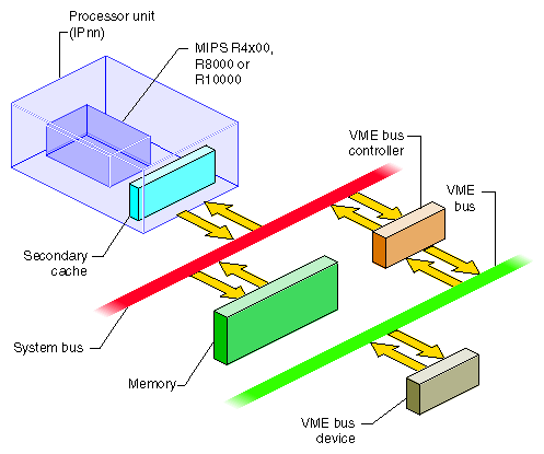
A VME bus controller is attached to the system bus to act as a bridge between the system bus and the VME bus. This arrangement is shown in Figure 14-1.
On the system bus, the VME bus controller acts as an I/O device. On the VME bus, the bus controller acts as a VME bus master. The VME controller has several tasks. Its most important task is mapping; that is, translating some range of physical addresses in the system address space to a range of VME bus addresses. The VME controller performs a variety of other duties for different kinds of VME access.
During programmed I/O (PIO) to the VME bus, software in the CPU loads or stores the contents of CPU registers to a device on the VME bus. The operation of a CPU load from a VME device register is as follows:
The CPU executes a load from a system physical address.
The system recognizes the physical address as one of its own.
The system translates the physical address into a VME bus address.
Acting as a VME bus master, the system starts a read cycle on the VME bus.
A slave device on the VME bus responds to the VME address and returns data.
The VME controller initiates a system bus cycle to return the data packet to the CPU, thus completing the load operation.
A store to a VME device is similar except that it performs a VME bus write, and no data is returned.
PIO input requires two system bus cycles—one to request the data and one to return it—separated by the cycle time of the VME bus. PIO output takes only one system bus cycle, and the VME bus write cycle run concurrently with the next system bus cycle. As a result, PIO input always takes at least twice as much time as PIO output.
On a Challenge L or Onyx system, the maximum rate of PIO output is approximately 750K writes per second. The maximum rate of PIO input is approximately 250K reads per second. The corresponding data rate depends on the number of bytes transferred on each operation, as summarized in Table 14-1.
Table 14-1. VME Bus PIO Bandwidth
Data Unit Size | Read | Write |
|---|---|---|
D8 | 0.25 MB/second | 0.75 MB/second |
D16 | 0.5 MB/second | 1.5 MB/second |
D32 | 1 MB/second | 3 MB/second |
| Note: The numbers in Table 14-1 were obtained by doing continuous reads, or continuous writes, to a device in the Challenge chassis. When reads and writes alternate, add approximately 1 microsecond for each change of direction. The use of a repeater to extend to an external card cage would add 200 nanoseconds or more to each transfer. |
A VME device that can act as a bus master can perform DMA into memory. The general sequence of operations in this case is as follows:
Kernel software uses PIO to program device registers of the VME device, telling it to perform DMA to a certain VME bus address for a specified length of data.
The VME bus master initiates the first read, write, block-read, or block-write cycle on the VME bus.
The VME controller, responding as a slave device on the VME bus, recognizes the VME bus address as one that corresponds to a physical memory address in the system.
If the bus master is writing, the VME controller accepts the data and initiates a system bus cycle to write the data to system memory.
If the bus master is reading, the VME controller uses a system bus cycle to read data from system memory, and returns the data to the bus master.
The bus master device continues to use the VME controller as a slave device until it has completed the DMA transfer.
During a DMA transaction, the VME bus controller operates independently of any CPU. CPUs in the system execute software concurrently with the data transfer. Since the system bus is faster than the VME bus, the data transfer takes place at the maximum data rate that the VME bus master can sustain.
In the Challenge and Onyx lines, the VME controller contains a “DMA Engine” that can be programmed to perform DMA-type transfers between memory and a VME device that is a slave, not a bus master.
The general course of operations in a DMA engine transfer is as follows:
The VME bus controller is programmed to perform a DMA transfer to a certain physical address for a specified amount of data from a specified device address in VME address space.
The VME bus controller, acting as the VME bus master, initiates a block read or block write to the specified device.
As the slave device responds to successive VME bus cycles, the VME bus controller transfers data to or from memory using the system bus.
The DMA engine transfers data independently of any CPU, and at the maximum rate the VME bus slave can sustain. In addition, the VME controller collects smaller data units into blocks of the full system bus width, minimizing the number of system bus cycles needed to transfer data. For both these reasons, DMA engine transfers are faster than PIO transfers for all but very short transfer lengths.
The maximum performance of the DMA engine for D32 transfers is summarized in Table 14-2. Performance with D64 Block transfers is somewhat less than twice the rate shown in Table 14-2. Transfers for larger sizes are faster because the setup time is amortized over a greater number of bytes.
Table 14-2. VME Bus Bandwidth, DMA Engine, D32 Transfer
Transfer Size | Read | Write | Block Read | Block Write |
|---|---|---|---|---|
32 | 2.8 MB/sec | 2.6 MB/sec | 2.7 MB/sec | 2.7 MB/sec |
64 | 3.8 MB/sec | 3.8 MB/sec | 4.0 MB/sec | 3.9 MB/sec |
128 | 5.0 MB/sec | 5.3 MB/sec | 5.6 MB/sec | 5.8 MB/sec |
256 | 6.0 MB/sec | 6.7 MB/sec | 6.4 MB/sec | 7.3 MB/sec |
512 | 6.4 MB/sec | 7.7 MB/sec | 7.0 MB/sec | 8.0 MB/sec |
1024 | 6.8 MB/sec | 8.0 MB/sec | 7.5 MB/sec | 8.8 MB/sec |
2048 | 7.0 MB/sec | 8.4 MB/sec | 7.8 MB/sec | 9.2 MB/sec |
4096 | 7.1 MB/sec | 8.7 MB/sec | 7.9 MB/sec | 9.4 MB/sec |
| Note: The throughput that can be achieved in VME DMA is very sensitive to several factors: |
The other activity on the VME bus.
The blocksize (larger is better).
Other overhead in the loop requesting DMA operations.
The loop used to generate the figures in Table 14-2 contained no activity except calls to dma_start().
the response time of the target VME board to a read or write request, in particular the time from when the VME adapter raises Data Strobe (DS) and the time the slave device raises Data Acknowledge (DTACK).
For example, if the slave device takes 500 ns to raise DTACK, there will always be fewer than 2 M data transfers per second.
Devices on the VME bus exist in one of the following address spaces:
The 16-bit space (A16) contains numbers from 0x0000 to 0xffff.
The 24-bit space (A24) contains numbers from 0x00 0000 to 0xff ffff.
The 32-bit space (A32) uses numbers from 0x0000 0000 to 0xffff ffff.
The 64-bit space (A64), defined in the revision D specification, uses 64-bit addresses.
The system bus also uses 32-bit or 64-bit numbers to address memory and other I/O devices on the system bus. In order to avoid conflicts between the meanings of address numbers, certain portions of the physical address space are reserved for VME use. The VME address spaces are mapped, that is, translated, into these ranges of physical addresses.
The translation is performed by the VME bus controller: It recognizes certain physical addresses on the system bus and translates them into VME bus addresses; and it recognizes certain VME bus addresses and translates them into physical addresses on the system bus.
Even with mapping, the entire A32 or A64 address space cannot be mapped into the physical address space. As a result, the system does not provide access to all of the VME address spaces. Only parts of the VME address spaces are available at any time.
In a user-level program you can perform PIO and certain types of DMA operations (see Chapter 4, “User-Level Access to Devices”), but you do not program these in terms of the physical addresses mapped to the VME bus. Instead, you call on the services of a kernel-level device driver to map a portion of VME address space into the address space of your process. The requested segment of VME space is mapped dynamically to a segment of your user-level address space—a segment that can differ from one run of the program to the next.
In a kernel-level device driver, you program PIO and DMA operations in terms of specific addresses in kernel space—memory addresses that are mapped to specified addresses in the VME bus address space. The mapping is either permanent, established by the system hardware, or dynamic, set up temporarily by a kernel function.
| Note: The remainder of this chapter has direct meaning only for kernel-level drivers, which must deal with physical mappings of VME space. |
The addressing needs of PIO access and DMA access are different.
PIO deals in small amounts of data, typically single bytes or words. PIO is directed to device registers that are identified with specific VME bus addresses. The association between a device register and its bus address is fixed, typically by setting jumpers or switches on the VME card.
DMA deals with extended segments of kilobytes or megabytes. The addresses used in DMA are not fixed in the device, but are programmed into it just before the data transfer begins. For example, a disk controller device can be programmed to read a certain sector and to write the sector data to a range of 512 consecutive bytes in the VME bus address space. The programming of the disk controller is done by storing numbers into its registers using PIO. While the registers respond only to fixed addresses that are configured into the board, the address to which the disk controller writes its sector data is just a number that is programmed into it each time a transfer is to start.
The key differences between addresses used by PIO and those used for DMA are:
PIO addresses are relatively few in number and cover small spans of data, while DMA addresses can span large ranges of data.
PIO addresses are closely related to the hardware architecture of the device and are configured by hardware or firmware, while DMA addresses are simply parameters programmed into the device before each operation.
In Challenge and Onyx systems, all VME mappings are dynamic, assigned as needed. Kernel functions are provided to create and release mappings between designated VME addresses and kernel addresses.
The Challenge and Onyx systems and their Power versions support from one to five VME buses. It is impossible to fit adequate segments of five separate A16, A24, and A32 address spaces into fixed mappings in the 40-bit physical address space available in these systems.
The VME controller in Challenge and Onyx systems uses programmable mappings. The IRIX kernel can program the mapping of twelve separate 8 MB “windows” on VME address space on each bus (a total of 96 MB of mapped space per bus). The kernel sets up VME mappings by setting the base addresses of these windows as required. A kernel-level VME device driver asks for and uses PIO mappings through the functions documented in “Mapping PIO Addresses” on page 325. Mapping PIO Addresses
A PIO map is a system object that represents the mapping from a location in the kernel's virtual address space to some small range of addresses on a VME or EISA bus. After creating a PIO map, a device driver can use it in the following ways:
Use the specific kernel virtual address that represents the device, either to load or store data, or to map that address into user process space.
Copy data between the device and memory without learning the specific kernel addresses involved.
Perform bus read-modify-write cycles to apply Boolean operators efficiently to device data.
The kernel virtual address returned by PIO mapping is not a physical memory address and is not a bus address. The kernel virtual address and the VME or EISA bus address need not have any bits in common.
The functions used with PIO maps are summarized in Table 14-3.
Table 14-3. Functions to Create and Use PIO Maps
Function | Header Files | Can Sleep | Purpose |
|---|---|---|---|
pio_mapalloc(D3) | pio.h & types.h | Y | Allocate a PIO map. |
pio_mapfree(D3) | pio.h & types.h | N | Free a PIO map. |
pio_badaddr(D3) | pio.h & types.h | N | Check for bus error when reading an address. |
pio_badaddr_val(D3) | pio.h & types.h | N | Check for bus error when reading an address and return the value read. |
pio_wbadaddr(D3) | pio.h & types.h | N | Check for bus error when writing to an address. |
pio_wbadaddr_val(D3) | pio.h & types.h | N | Check for bus error when writing a specified value to an address. |
pio_mapaddr(D3) | pio.h & types.h | N | Convert a bus address to a virtual address. |
pio_bcopyin(D3) | pio.h & types.h | Y | Copy data from a bus address to kernel's virtual space. |
pio_bcopyout(D3) | pio.h & types.h | Y | Copy data from kernel's virtual space to a bus address. |
pio_andb_rmw(D3) | pio.h & types.h | N | Byte read-and-write. |
pio_andh_rmw(D3) | pio.h & types.h | N | 16-bit read-and-write. |
pio_andw_rmw(D3) | pio.h & types.h | N | 32-bit read-and-write. |
pio_orb_rmw(D3) | pio.h & types.h | N | Byte read-or-write. |
pio_orh_rmw(D3) | pio.h & types.h | N | 16-bit read-or-write. |
pio_orw_rmw(D3) | pio.h & types.h | N | 32-bit read-or-write. |
A kernel-level device driver creates a PIO map by calling pio_mapalloc(). This function performs memory allocation and so can sleep. PIO maps are typically created in the pfxedtinit() entry point, where the driver first learns about the device addresses from the contents of the edt_t structure (see “Entry Point edtinit()” in Chapter 7).
The parameters to pio_mapalloc() describe the range of addresses that can be mapped in terms of
the bus type, ADAP_VME or ADAP_EISA from sys/edt.h
the bus number, when more than one bus is supported
the address space, using constants such as PIOMAP_A24N or PIOMAP_EISA_IO from sys/pio.h
the starting bus address and a length
This call also specifies a “fixed” or “unfixed” map. The usual type is “fixed.” For the differences, see “Fixed PIO Maps” and “Unfixed PIO Maps”.
A call to pio_mapfree() releases a PIO map. PIO maps created by a loadable driver must be released in the pfxunload() entry point (see “Entry Point unload()” in Chapter 7 and “Unloading” in Chapter 9).
The PIO map is created from the parameters that are passed. These are not validated by pio_mapalloc(). If there is any possibility that the mapped device is not installed, not active, or improperly configured, you should test the mapped address.
The pio_badaddr() and pio_badaddr_val() functions test the mapped address to see if it is usable for input. Both functions perform the same operation: operating through a PIO map, they test a specified bus address for validity by reading 1, 2, 4, or 8 bytes from it. The pio_badaddr_val() function returns the value that it reads while making the test. This can simplify coding, as shown in Example 14-1.
Example 14-1. Comparing pio_badaddr() to pio_badaddr_val()
unsigned int gotvalue;
piomap_t *themap;
/* Using only pio_badaddr() */
   if (!pio_badaddr(themap,CTLREG,4)
   {
      (void) pio_bcopyin(themap,CTLREG,&gotvalue,4,4,0);
      ...use "gotvalue"
/* Using pio_badaddr_val() */
   if (!pio_badaddr_val(themap,CTLREG,4,&gotvalue))
   {
      ...use "gotvalue"
|
The pio_wbadaddr() function tests a mapped device address for writability. The pio_wbadaddr_val() not only tests the address but takes a specific value to write to that address in the course of testing it.
From a fixed PIO map you can recover a kernel virtual address that corresponds to the first bus address in the map. The pio_mapaddr() function is used for this.
You can use this address to load or store data into device registers. In the pfxmap() entry point (see “Concepts and Use of mmap()” in Chapter 7), you can use this address with the v_mapphys() function to map the range of device addresses into the address space of a user process.
You cannot extract a kernel address from an unfixed PIO map, as explained under “Unfixed PIO Maps”.
You can apply a variety of kernel functions to any PIO map, fixed or unfixed. The pio_bcopyin() and pio_bcopyout() functions copy a range of data between memory and a fixed or unfixed PIO map. These functions are optimized to the hardware that exists, and they do all transfers in the largest size possible (32 or 64 bits per transfer). If you must transfer data in specific sizes of 1 or 2 bytes, use direct loads/stores to mapped addresses.
The series of functions pio_andb_rmw() and pio_orb_rmw() perform a read-modify-write cycle on the VME bus. You can use them to set or clear bits in device registers. A read-modify-write cycle is faster than a load followed by a store since it uses fewer system bus cycles.
On a Challenge or Onyx system, a PIO map can be either “fixed” or “unfixed.” This attribute is specified when the map is created.
The Challenge and Onyx architecture provides for a total of 15 separate, 8 MB windows on VME address space for each VME bus. Two of these are permanently reserved to the kernel, and one window is reserved for use with unfixed mappings. The remaining 12 windows are available to implement fixed PIO maps.
When the kernel creates a fixed PIO map, the map is associated with one of the 12 available VME mapping windows. The kernel tries to be clever, so that whenever a PIO map falls within an 8 MB window that already exists, the PIO map uses that window. If the desired VME address is not covered by an open window, one of the twelve windows for that bus is opened to expose a mapping for that address.
It is possible in principle to configure thirteen devices that are scattered so widely in the A32 address space that twelve, 8 MB windows cannot cover all of them. In that unlikely case, the attempt to create the thirteenth fixed PIO map will fail for lack of a mapping window.
In order to prevent this, simply configure your PIO addresses into a span of at most 96 MB per bus (see “Configuring Device Addresses”).
When you create an unfixed PIO map, the map is not associated with any of the twelve mapping windows. As a result, the map cannot be queried for a kernel address that might be saved, or mapped into user space.
You can use an unfixed map with kernel functions that copy data or perform read-modify-write cycles. These functions use the one mapping window that is reserved for unfixed maps, repositioning it in VME space if necessary.
The lboot command uses an unfixed map to perform the probe and exprobe sequences from VECTOR statements (see “Configuring the System Files”). As a result, these probes do not tie up mapping windows.
DMA is supported only for the A24 and A32 address spaces. DMA addresses are always assigned dynamically in the Challenge and Onyx systems.
A DMA map is a system object that represents a mapping between a buffer in kernel virtual space and a range of VME bus addresses. After creating a DMA map, a driver uses the map to specify the target address and length to be programmed into a VME bus master before a DMA transfer.
The functions that operate on DMA maps are summarized in Table 14-4.
Table 14-4. Functions That Operate on DMA Maps
Function | Header Files | Can Sleep | Purpose |
|---|---|---|---|
dma_map(D3) | dmamap.h & types.h & sema.h | N | Load DMA mapping registers for an imminent transfer. |
dma_mapbp(D3) | dmamap.h & types.h & sema.h | N | Load DMA mapping registers for an imminent transfer. |
dma_mapaddr(D3 ) | dmamap.h & types.h & sema.h | N | Return the “bus virtual” address for a given map and address. |
dma_mapalloc(D3 ) | dmamap.h & types.h & sema.h | Y | Allocate a DMA map. |
dma_mapfree(D3) | dmamap.h & types.h & sema.h | N | Free a DMA map. |
vme_adapter(D3) | vmereg.h & types.h | N | Determine VME adapter that corresponds to a given memory address. |
A device driver allocates a DMA map using dma_mapalloc(). This is typically done in the pfxedtinit() entry point, provided that the maximum I/O size is known at that time (see “Entry Point edtinit()” in Chapter 7). The important argument to dma_mapalloc() is the maximum number of pages (I/O pages, the unit is IO_NBPP declared in sys/immu.h) to be mapped at one time.
DMA maps created by a loadable driver should be released in the pfxunload() entry point (see “Entry Point unload()” in Chapter 7 and “Unloading” in Chapter 9).
A DMA map is used prior to a DMA transfer into or out of a buffer in kernel virtual space. The function dma_map() takes a DMA map, a buffer address, and a length. It assigns a span of contiguous VME addresses of the specified length, and sets up a mapping between that range of VME addresses and the physical addresses that represent the specified buffer.
When the buffer spans two or more physical pages (IO_NBPP units), dma_map() sets up a scatter/gather operation, so that the VME bus controller will place the data in the appropriate page frames.
It is possible that dma_map() cannot map the entire size of the buffer. This can occur only when the buffer spans two or more pages, and is caused by a shortage of mapping registers in the bus adapter. The function maps as much of the buffer as it can, and returns the length of the mapped data. You must always anticipate that dma_map() might map less than the requested number of bytes, so that the DMA transfer has to be done in two or more operations.
Following the call to dma_map(), you call dma_mapaddr() to get the bus virtual address that represents the first byte of the buffer. This is the address you program into the bus master device (using a PIO store), in order to set its starting transfer address. Then you initiate the DMA transfer (again by storing a command into a device register using PIO).
To install a VME device in a Challenge or Onyx system, you need to configure the device itself to respond to PIO addresses in a supported range of VME bus addresses, and you need to inform IRIX of the device addresses.
Normally a VME card can be programmed to use different VME addresses for PIO, based on jumper or switch settings on the card. The devices on a single VME bus must be configured to use unique addresses. Errors that are hard to diagnose can arise when multiple cards respond to the same bus address. Devices on different VME buses can use the same addresses. Not all parts of each address space are accessible. The accessible parts are summarized in Table 14-5.
Table 14-5. Accessible VME Addresses in Challenge and Onyx Systems
Address Space | Challenge and Onyx Systems |
|---|---|
A16 | All |
A24 | 0x80 0000–0xFF FFFF |
A32 | 0x0000 0000–0x7FFF FFFF (maximum of 96 MB in 8 MB units) |
Within the accessible ranges, certain VME bus addresses are used by VME devices. You can find these addresses documented in the /var/sysgen/system/irix.sm file. You must configure OEM devices to avoid the addresses used by Silicon Graphics devices that are installed on the same system.
Finally, on the Challenge and Onyx systems, take care to cluster PIO addresses in the A32 space so that they occupy at most a 96 MB span of addresses. The reasons are explained under “Fixed PIO Maps”.
Inform IRIX and the device driver of the existence of a VME device by adding a VECTOR statement to a file in the directory /var/sysgen/system (see “Kernel Configuration Files” in Chapter 2). The syntax of a VECTOR statement is documented in two places:
The /var/sysgen/system/irix.sm file itself contains descriptive comments on the syntax and meaning of the statement, as well as numerous examples.
The system(4) reference page gives a more formal definition of the syntax.
In addition to the VECTOR statement, you may need to code an IPL statement.
The important elements in a VECTOR line are as follows:
bustype | Specified as VME for VME devices. The VECTOR statement can be used for other types of buses as well. |
module | The base name of the device driver for this device, as used in the /var/sysgen/master.d database (see “Master Configuration Database” in Chapter 2 and “How Names Are Used in Configuration” in Chapter 9 ). |
adapter | The number of the VME bus where the device is attached—the bus number in a Challenge or Onyx machine. |
ipl | The interrupt level at which the device causes interrupts, from 0 to 7. |
vector | An 8-bit value between 1 and 254 that the device returns during an interrupt acknowledge cycle. |
ctlr | The “controller” number is simply an integer parameter that is passed to the device driver at boot time. It can be used for example to specify a logical unit number. |
iospace, iospace2, iospace3 | Each iospace group specifies the VME address space, the starting bus address, and the size of a segment of VME address space used by this device. |
probe or exprobe | Specify a hardware test that can be applied at boot time to find out if the device exists. |
Use the probe or exprobe parameter to program a test for the existence of the device at boot time. If the device does not respond (because it is offline or because it has been removed from the system), the lboot command will not invoke the device driver for this device.
The device driver specified by the module parameter is invoked at its pfxedtinit() entry point, where it receives most of the other information specified in the VECTOR statement (see “Entry Point edtinit()” in Chapter 7).
Omit the vector parameter in either of two cases: when the device does not cause interrupts, or when it supports a programmable interrupt vector (see “Allocating an Interrupt Vector Dynamically”).
Use the iospace parameters to pass in the exact VME bus addresses that correspond to this device, as configured in the device. Up to three address space ranges can be passed to the driver. This does not restrict the device—it can use other ranges of addresses, but the device driver has to deduce their addresses from other information. The device driver typically uses this data to set up PIO maps (see “PIO Addressing in Challenge and Onyx Systems”)
In a Challenge or Onyx system, you can direct VME interrupts to specific CPUs. This is done with the IPL statement, also written into a file in /var/sysgen/system. The IPL statement, which like the VECTOR statement is documented in both the system(4) reference page and the /var/sysgen/system/irix.sm file itself, has only two parameters:
level | The VME interrupt level to be directed, 0 to 7 (the same value that is coded as ipl= in the VECTOR statement. |
cpu | The number of the CPU that should handle all VME interrupts at this level. |
The purpose of the IPL statement is to send interrupts from specific devices to a specific CPU. There are two contradictory reasons for doing this:
That CPU is dedicated to handling those interrupts with minimum latency
Those interrupts would disrupt high-priority work being done on other CPUs if they were allowed to reach the other CPUs.
The IPL statement cannot direct interrupts from a specific device; it directs all interrupts that occur at the specified level.
When a VME device generates an interrupt, the Silicon Graphics VME controller initiates an interrupt acknowledge (IACK) cycle on the VME bus. During this cycle, the interrupting device presents a data value that characterizes the interrupt. This is the interrupt vector, in VME terminology.
According to the VME standard, the interrupt vector can be a data item of 8, 16, or 32 bits. However, Challenge and Onyx systems accept only an 8-bit vector, and its value must fall in the range 1-254 inclusive. (0x00 and 0xFF are excluded because they could be generated by a hardware fault.)
The interrupt vector returned by some VME devices is hard-wired or configured into the board with switches or jumpers. When this is the case, the vector number should be written as the vector parameter in the VECTOR statement that describes the device (see “Configuring the System Files”).
Some VME devices are programmed with a vector number at runtime. For these devices, you omit the vector parameter, or give its value as an asterisk. In the device driver, you use the functions in Table 14-6 to choose a vector number.
Table 14-6. Functions to Manage Interrupt Vector Values
Function | Header Files | Can Sleep | Purpose |
|---|---|---|---|
vme_ivec_alloc(D3) | vmereg.h & types.h | N | Allocate a VME bus interrupt vector. |
vme_ivec_free(D3) | vmereg.h & types.h | N | Free a VME bus interrupt vector. |
vme_ivec_set(D3) | vmereg.h & types.h | N | Register a VME bus interrupt vector. |
In the pfxedtinit() entry point, the device driver selects a vector number for the device to use. The best way to select a number is to call vme_ivec_alloc(), which returns a number that has not been registered for that bus, either dynamically or in a VECTOR line.
The driver then uses vme_ivec_set() to register the chosen vector number. This function takes parameters that specify
The vector number
The bus number to which it applies
The address of the interrupt handler for this vector—typically but not necessarily the name of the pfxintr() entry point of the same driver
An integer value to be passed to the interrupt entry point—typically but not necessarily the vector number
The vme_ivec_set() function simply registers the number in the kernel, with the following two effects:
The vme_ivec_alloc() function does not return the same number to another call until the number is released.
The specified handler is called when any device presents this vector number on an interrupt.
Multiple devices can present the identical vector, provided that the interrupt handler has some way of distinguishing one device from another.
| Note: If you are working with both the VME and EISA interfaces, it is worth noting that the number and types of arguments of vme_ivec_set() differ from the similar EISA support function eisa_ivec_set(). |
There is a limit of 254 vector numbers per bus, so it is a good idea for a loadable driver, in its pfxunload() entry point, to release a vector by calling vme_ivec_free() (see “Entry Point unload()” in Chapter 7 and “Unloading” in Chapter 9).
A common problem with programmable vectors in the Challenge or Onyx systems is the appearance of the following warning in the SYSLOG file:
Warning: Stray VME interrupt: vector =0xff |
One possible cause of this error is that the board is emitting the wrong interrupt vector; another is that the board is emitting the correct vector but with the wrong timing, so that the VME bus adapter samples all-binary-1 instead. Both these conditions can be verified with a VME bus analyzer. In the Challenge or Onyx hardware design, the most likely cause is the presence of empty slots in the VME card cage. All empty slots must be properly jumpered in order to pass interrupts correctly.
The overview topic, “VME Bus in Challenge and Onyx Systems”, provides sufficient orientation for most users of VME devices. However, if you are designing hardware or a high-performance device driver specifically for the Challenge and Onyx systems, the details in this topic are important.
| Note: For information on physical cabinets, panels, slot numbering, cables and jumpers, and data about dimensions and airflow, refer to the Owner's Guide manual for your machine. For example, see the POWER CHALLENGE AND CHALLENGE XL Rackmount Owner's Guide (007-1735) for the physical layout and cabling of VME busses in the large Challenge systems. |
The VME bus interface circuitry for Challenge and Onyx systems resides on a mezzanine board called the VMEbus Channel Adapter Module (VCAM) board. One VCAM board is standard in every system and mounts directly on top of the IO4 board in the system card cage.
The IO4 board is the heart of the I/O subsystem. The IO4 board supplies the system with a basic set of I/O controllers and system boot and configuration devices such as serial and parallel ports, and Ethernet.
In addition, the IO4 board provides these interfaces:
two Flat Cable Interconnects (FCIs) for connection to Card Cage 3 (CC3)
two SCSI-2 cable connections
two Ibus connections
A Challenge or Onyx system can contain multiple IO4 boards, which can operate in parallel. (Early versions of the IO4 have a possible hardware problem that is described in Appendix B, “Challenge DMA with Multiple IO4 Boards”.)
The main set of buses in the Challenge and Onyx system architecture is the Everest address and data buses, Ebus for short. The Ebus provides a 256-bit data bus and a 40-bit address bus that can sustain a bandwidth of 1.2 GB per second.
The 256-bit data bus provides the data transfer capability to support a large number of high-performance RISC CPUs. The 40-bit address bus is also wide enough to support 16 GB of contiguous memory in addition to an 8 GB I/O address space.
The 64-bit Ibus (also known as the HIO bus) is the main internal bus of the I/O subsystem and interfaces to the high-power Ebus through a group of bus adapters.The Ibus has a bandwidth of 320 MB per second that can sufficiently support a graphics subsystem, a VME64 bus, and as many as eight SCSI channels operating simultaneously.
Communication with the VME and SCSI buses, the installed set or sets of graphics boards, and Ethernet takes place through the 64-bit Ibus. The Ibus interfaces to the main system bus, the 256-bit Ebus, through a set of interface control devices, an I address (IA) and four I data (ID). The ID ASICs latch the data, and the IA ASIC clocks the data from each ID to the Flat Cable Interface (FCI) through the F controller (or F chip).
Two FCI controllers (or F controllers) help handle the data transfers to and from an internal graphics board set (if present) and any VMEbus boards in optional CC3 applications. The SCSI-2 (S1) controller serves as an interface to the various SCSI-2 buses. The Everest peripheral controller (EPC) device manages the data movement to and from the Ethernet, a parallel port, and various types of on-board PROMs and RAM.
The worst-case delay for the start of a VME access, if all of the devices on the IO4 simultaneously request the IO channel for a 128 byte write and the VME adapter receives the grant last, the VME access start could be delayed for a total of about 2 microseconds. Only a VME read would suffer this delay; a VME write would not.
There is a another potential delay from an independent cause, which depends on the number of bus master (IO4 and CPU) boards on the system bus. If all the E-bus masters in a fairly large configuration hit the bus at once, a VME read or write could be held up by as much as 1 microsecond in a large system.
The Challenge and Onyx systems support up to five independent VME buses in a single system. The numbering of these buses is not sequential.
There is always a VME bus number 0. This is the bus connected to the system midplane. It is always connected by the primary IO4 board (the IO4 board attached to the highest slot on the system bus). Bus numbers for other VME buses depend on the Ebus slot number where their IO4 is attached, and on the I/O adapter number of the VCAM card on the IO4. Each IO4 board supports adapter numbers from 1 to 7, but a VME bus can only be attached to adapter number 2, 3, 5, or 6. These four adapters are given VME index numbers of 0, 1, 2, and 3 respectively.
The bus number of a VME bus is given by E*4+A, where E is the Ebus slot of the IO4 card, and A is the index of the adapter on the IO4. A VME bus attached through adapter 3 on the IO4 in Ebus slot 13 is bus number 53, from the sum of adapter index 1 and 4 times the slot number.
The VCAM board provides the interface between the Ebus and the VMEbus and manages the signal level conversion between the two buses. The VCAM also provides a pass-through connection that ties the graphics subsystem to the Ebus. The VCAM can operate as either a master or a slave. It supports DMA-to-memory transactions on the Ebus and programmed I/O (PIO) operations from the system bus to addresses on the VMEbus. In addition, the VCAM provides virtual address translation capability and a DMA engine that increases the performance of non-DMA VME boards.
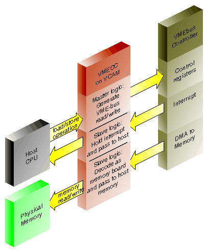
The VMECC (VME cache controller) gate array is the major active device on the VCAM. The VMECC interfaces and translates host CPU operations to VMEbus operations (see Figure 14-2). The VMECC also decodes VMEbus operations to translate for the host side.
The VMECC provides the following features:
an internal DMA engine to speed copies between physical memory and VME space (see “Operation of the DMA Engine”)
a 16-entry deep PIO FIFO to smooth writing to the VME bus from the host CPUs
a built-in VME interrupt handler and built-in VME bus arbiter
an explicit internal delay register to aid in spacing PIOs for VME controller boards that cannot accept back-to-back operations
support for issuing A16, A24, A32, and A64 addressing modes as a bus master during PIO
support for single-item transfers (D8, D16, D32, and D64) as bus master during PIO
support for response as a slave to A24, A32, and A64 addressing modes to provide DMA access to the Ebus
support for single-item transfers (D8, D16, and D32) as a slave during DMA access to the Ebus
support for block item transfers (D8, D16, D32, and D64) as a slave during DMA access to the Ebus
The VMECC also provides four levels of VMEbus request grants, 0-3 (3 has the highest priority), for DMA arbitration. Do not confuse these bus request levels with the interrupt priority levels 1-7. Bus requests prioritize the use of the physical lines representing the bus and are normally set by means of jumpers on the interface board.
Data transfers between VME controller boards and the host CPU(s) takes place through the VMECC on the VCAM board, then through a flat cable interface (FCI), and onto the F controller ASIC.
The F controller acts as an interface between the Ibus and the Flat Cable Interfaces (FCIs). This device is primarily composed of FIFO registers and synchronizers that provide protocol conversion and buffer transactions in both directions and translate 34-bit I/O addresses into 40-bit system addresses.
Two configurations of the F controller are used on the IO4 board; the difference between them is the instruction set they contain. One version is programmed with a set of instructions designed to communicate with the GFXCC (for graphics); the other version has instructions designed for the VMECC. All communication with the GFXCC or VMECC ICs is done over the FCI, where the F controller is always the slave. Both versions of F controller ASICs have I/O error-detection and handling capabilities. Data errors that occur on either the Ibus or the FCI are recorded by the F controller and sent to the VMECC or GFXCC.
ICs must report an error to the appropriate CPU and log any specific information about the operation in progress. FCI errors are recorded in the error status register, which provides status of the first error that occurred, and the cause of the most recent FCI reset.
The VME bus supports seven levels of prioritized interrupts, 1 through 7 (where 7 has the highest priority). The VMECC has a register associated with each level. When the system responds to the VMEbus interrupt, it services all devices identified in the interrupt vector register in order of their VMEbus priority (highest number first).
The following list outlines how a VMEbus interrupt is generated:
A VME controller board asserts a VME interrupt on one of the IRQ levels.
The built-in interrupt handler in the VMECC chip checks if the interrupt level is presently enabled by an internal interrupt mask.
The interrupt handler in the VMECC issues a bussed IACK (interrupt acknowledge) response and acquires the vector from the device. The 3-bit response identifies one of the seven VME levels.
If multiple VME boards are present, the bussed IACK signal is sent to the first VME controller as an IACKIN. When the first controller is not the requesting master, it passes the IACKIN signal to the next board (in the daisy-chain) as IACKOUT.
The requesting board responds to IACKIN by issuing a DTACK* (data acknowledge signal), blocking the IACKOUT signal to the next board, and placing an 8-bit interrupt vector number on the data bus.
The VMECC latches the interrupt vector, and an interrupt signal is sent over the FCI interface to the F-chip and is queued awaiting completion of other F-chip tasks.
The F controller ASIC requests the I-bus and sends the interrupt to the IA chip.
The IA chip requests the Ebus and sends the interrupt over the Ebus to the CC chip on the IP19/IP21 board.
The CC chip interrupts an R4400/R8000, provided the interrupt level is not masked.
The time for this to complete is normally less than 3 microseconds, but will be queued to await completion of other VME activities.
The Challenge and Onyx VME interface supports all protocols defined in Revision C of the VME specification plus the A64 and D64 modes defined in Revision D. The D64 mode allows DMA bandwidths of up to 60 MB. This bus also supports the following features:
seven levels of prioritized processor interrupts
16-bit, 24-bit, and 32-bit data addresses and 64-bit memory addresses
16-bit and 32-bit accesses (and 64-bit accesses in MIPS III mode)
8-bit, 16-bit, 32-bit, and 64-bit data transfer
DMA to and from main memory
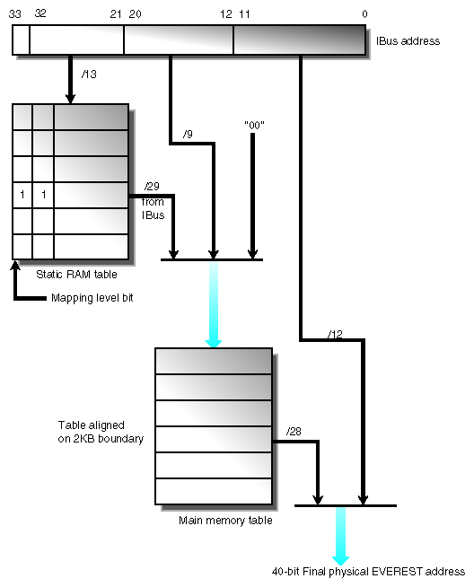
In the Challenge and Onyx series, a DMA address from a VME controller goes through a two-level translation to generate an acceptable physical address. This requires two levels of mapping. The first level of mapping is done through the map RAM on the IO4 board. The second level is done through the map tables in system memory. This mapping is shown in Figure 14-3.
| Note: The second level mapping requires system memory to be reserved for the mapping tables. The current limit on the number of pages that is allocated for map tables is 16 pages and the maximum memory allotted for the map tables is 64 KB. The R4400 provides a 4 KB page size for 16 pages (4 KB * 16 pages= 64 KB). The R8000 provides a 16 KB page size for 4pages (16 KB * 4 pages = 64 KB). |
Each second-level map table entry corresponds to 4 KB of physical memory. In addition, each second-level map table entry is 4 bytes. With 64 KB of mapping table, there are a total of 16 K entries translating a maximum of 64 MB of DMA mapping, setting a limit of 64 MB that can be mapped at any time for each VME bus. This does not set any limit on the amount of DMA that can be done by a board during its operation.
Referring to the top of Figure 14-3, bits 32 and 33 from the IBus address come from the VMECC. These two bits determine a unique VMEbus number for systems with multiple VME buses. Of the remaining 32 bits (31 to 0), 12 are reserved for an offset in physical memory, and the other 20 bits are used to select up to 220 or 1 million pages into the main memory table. However, as stated earlier only 64 KB is allocated for map tables.
As shown in Figure 14-3, thirteen bits go to the static RAM table. Recall that two of the thirteen bits are from the VMECC to identify the VMEbus number. The static RAM table then generates a 29-bit identifier into the main memory table. These 29 bits select a table in the main memory table. An additional nine bits select an entry or element within the table. A 00 (two zeros) are appended to form a 40-bit address into the main memory table.
The main memory table then generates 28-bit address which is then appended to the 12-bit offset of the IBus to form the final 40-bit physical address.
Interrupts within the Challenge/Onyx architecture are managed by a set of interrupt vectors. An interrupt generated by an I/O device like a VME controller in turn generates an interrupt to the CPU on one of the previously assigned levels.
Each IRQ on each VME bus is assigned an internal interrupt level, and by default all these levels are at the same priority. If multiple interrupts arrive simultaneously within a single bus, for example IRQ 3 and IRQ 4 at once, priority is given to the higher-numbered IRQ.
All VME interrupts are made to go to CPU 0 (unless configured differently with IPL statements). This prevents one interrupt level from preempting the driver handling a different VME interrupt level.
When designing an OEM hardware board to interface to the Challenge or Onyx VME bus, observe the following restrictions:
Devices should require 8-bit interrupt vectors only. This is the only interrupt vector size that is supported by the VMECC or recognized by the IRIX kernel.
Devices must not require UAT (unaligned transfer or tri-byte) access.
Devices in slave mode must not require address modifiers other than Supervisory/Nonprivileged data access.
While in master mode, a device must use only nonprivileged data access or nonprivileged block transfers.
The Challenge or Onyx VME bus does not support VSBbus boards. In addition, there are no pins on the back of the VME backplane. This area is inaccessible for cables or boards.
Metal face plates or front panels on VME boards may prevent the I/O door from properly closing and can possibly damage I/O bulkhead. (In some VME enclosures, a face plate supplies required EMI shielding. However, the Challenge chassis already provides sufficient shielding, so these plates are not necessary.)
The following notes are related to the design of a VME bus master device to work with a machine in the Challenge/Onyx series. A VME bus master, when programmed using the functions described in “Mapping DMA Addresses”, can transfer data between itself and system memory.
The setup time at the start of a DMA transfer is as follows:
First word of a read is delivered to the master in 3 to 8 microseconds.
First word of a write is retrieved from the master in 1 to 3 microseconds.
The F controller does the mapping from A32 mode into system memory and automatically handles the crossing of page boundaries. The VME Bus Master is not required to make AS go high and then low on 4 KB boundaries. However, when using A64 addressing, the device may have to change the address on the 4 KB boundaries and cause a transition on AS low to high, and then back to low. This incurs new setup delays.
The important parts of the VME handshake cycle are diagrammed in Figure 14-4.
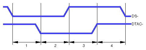
Intervals 1 and 3 represent the response latency in the bus slave (the VMECC). Intervals 2 and 4 represent the latency in the VME Bus Master. In the Challenge and Onyx systems,
part 1 is approximately 40 nanoseconds
part 3 is approximately 25 nanoseconds
The total contribution by the VMECC is approximately 65 nanoseconds. If the total of the four intervals can be held to 125 nanoseconds, the absolute peak transfer rate (in D64 mode) is 64 MB per second.
| Note: Startup and latency numbers are averages and may occasionally be longer. The system design does not have any guaranteed latency. |
The VME specification provides for a burst length of 265 bytes in D8, D16, and D32 modes, or 2 KB in D64. The burst length is counted in bytes, not transfer cycles.
Operating at this burst length, the duration of a single burst of 2 KB would be 256 transfers at 125 nanoseconds each, plus a startup of roughly 5 microseconds, giving a total of 37 microseconds per burst. Continuous, back-to-back bursts could achieve at most 55 MB per second.
However, the Challenge and Onyx VMECC uses a 20-bit burst counter allowing up to 2 MB in a burst of any data size. Suppose the bus master transfers 64 KB per burst, transferring 4-byte data words. The duration of a single burst would be 8,192 times 125 nanoseconds, plus 5 microseconds startup, or 1,029 microseconds per burst. Continuous bursts of this size achieve a data rate of 63.7 MB per second.
The use of long bursts violates the VME standard, and a bus master that depends on long bursts is likely not to work in other computers. If you decide to exceed the VME bus specifications, you should condition this feature with a field in a control register on the VME board, so that it can be disabled for use on other VME systems.