This chapter gives an overview of the management of physical and virtual memory in SGI systems based on the MIPS R5000 and R10000 processors. The purpose is to give you the background to understand terms used in device driver header files and reference pages, and to understand the limitations and special conventions used by some kernel functions.
This information is only of academic interest if you intend to control a device from a user-level process. (See Chapter 3, “Device Control Software”, for the difference between user-level and kernel-level drivers.) For a deeper level of detail on SGI Origin 2000 memory hardware, see the hardware manuals listed under “Additional Reading”.
The following main topics are covered in this chapter.
“CPU Access to Memory and Devices” summarizes the hardware architecture by which the CPU accesses memory.
“The 32-Bit Address Space” describes the parts of the physical address space when 32-bit addressing is used.
“The 64-Bit Address Space” describes the 64-bit physical address space.
“Address Space Usage in SGI Origin 2000 Systems” gives an overview of how physical memory is addressed in the complex architecture of the SGI Origin 2000.
Each SGI computer system has one or more CPU modules. A CPU reads data from memory or a device by placing an address on a system bus, and receiving data back from the addressed memory or device. An address can be translated more than once as it passes through multiple layers of bus adapters. Access to memory can pass through multiple levels of cache.
A CPU is a hardware module containing a MIPS processor chip such as the R8000, together with system interface chips and possibly a secondary cache. SGI CPU modules have model designation of the form IPnn; for example, the IP22 module is used in the Indy workstation. The CPU modules supported by IRIX 6.5 are listed in Table 1-1.
Table 1-1. CPU Modules and System Names
Module | MIPS Processor | System Families |
|---|---|---|
IP19 | R4x00 | Challenge (other than S model), Onyx |
IP20 | R4x00 | Indigo |
IP21 | R8000 | Power Challenge, Power Onyx |
IP22 | R4x00 | Indigo, Indy, Challenge S |
IP25 | R10000 | Power Challenge R10000 |
IP26 | R8000 | Power Indigo |
IP27 | R10000 | SGI Origin 2000 |
IP28 | R10000 | Power Indigo2 R10000 |
IP30 | R10000 | Octane |
IP32 | R10000 | O2 |
IP35 | R12000 | SGI Origin 3000 |
Modules with the same IP designation can be built in a variety of clock speeds, and they can differ in other ways. (For example, an IP27 can have 0, 1 or 2 R10000 modules plugged into it.) Also, the choice of graphics hardware is independent of the CPU model. However, all these CPUs are basically identical as seen from software.
At the interactive command line, you can determine which CPU module a system uses with the following command:
hinv -c processor |
Within a shell script, it is more convenient to process the terse output of
uname -m |
(See the uname(1) and hinv(1) reference pages.)
Within a program, you can get the CPU model using the getinvent() function. For an example, see “Testing the Inventory In Software” in Chapter 2.
The CPU generates the address of data that it needs—the address of an instruction to fetch, or the address of an operand of an instruction. It requests the data through a mechanism that is depicted in simplified form in Figure 1-1.
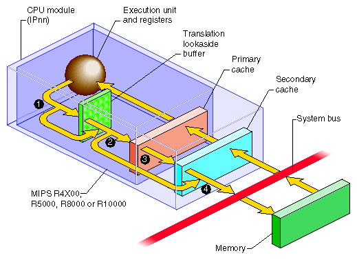
The address of the needed data is formed in the processor execution or instruction-fetch unit. Most addresses are then mapped from virtual to real through the Translation Lookaside Buffer (TLB). Certain ranges of addresses are not mapped, and bypass the TLB.
Most addresses are presented to the primary cache, a cache in the processor chip. If a copy of the data with that address is found, it is returned immediately. Certain address ranges are never cached; these addresses pass directly to the bus.
When the primary cache does not contain the data, the address is presented to the secondary cache. If it contains a copy of the data, the data is returned immediately. The size and the architecture of the secondary cache differ from one CPU model to another.
The address is placed on the system bus. The memory module that recognizes the address places the data on the bus.
The process in Figure 1-1 is correct for an SGI Origin 2000 system when the addressed data is in the local node. When the address applies to memory in another node, the address passes out through the connection fabric to a memory module in another node, from which the data is returned.
The MIPS processor under IRIX operates in one of two modes: kernel and user. The processor enters the more privileged kernel mode when an interrupt, a system instruction, or an exception occurs. It returns to user mode only with a “Return from Exception” instruction.
Certain instructions cannot be executed in user mode. Certain segments of memory can be accessed only in kernel mode, and other segments only in user mode.
The MIPS processor contains an array of Translation Lookaside Buffer (TLB) entries that map, or translate, virtual addresses to physical ones. Most memory accesses are first mapped by reference to the TLB. This permits the IRIX kernel to relocate parts of the kernel's memory and to implement virtual memory for user processes. The translation scheme is summarized in the following sections and covered in detail in the hardware manuals listed under “Additional Reading”.
Each TLB entry describes a segment of memory containing two adjacent pages. When the input address falls in a page described by a TLB entry, the TLB supplies the physical memory address for that page. The translated address, now physical instead of virtual, is passed on to the cache, as shown in Figure 1-1.
When the input address is not covered by any active TLB entry, the MIPS processor generates a “TLB miss” interrupt, which is handled by an IRIX kernel routine. The kernel routine inspects the address. When the address has a valid translation to some page in the address space, the kernel loads a TLB entry to describe that page, and restarts the instruction.
The size of the TLB is important for performance. The size of the TLB in different processors is shown in Table 1-2.
Table 1-2. Number of TLB Entries by Processor Type
Processor Type | Number of TLB Entries |
|---|---|
R4x00 | 96 |
R5000 | 96 |
R8000 | 384 |
R10000 | 128 |
R12000 | 128 |
There are not sufficient TLB entries to describe the entire address space of even a single process. The IRIX kernel creates a page table in kernel memory for each process. The page table contains one entry for each virtual memory page in the address space of that process. Whenever an executing program refers to an address for which there is no current TLB entry, the CPU traps to the TLB miss handler. The handler loads one TLB entry from the appropriate page table entry of the current process, in order to describe the needed virtual address. Then it resumes execution with the failed instruction.
In order to extend a virtual address space, the kernel takes the following two steps.
It allocates unused page table entries to describe the needed pages. This defines the virtual addresses the pages will have.
It allocates page frames in memory to contain the pages themselves, and puts their physical addresses in the page table entries.
When the CPU requests an invalid address—because the processor is in the wrong mode, or an address does not translate to a valid location in the address space, or an address refers to hardware that does not exist in the system—an addressing exception occurs. The processor traps to a particular address in the kernel.
An addressing exception can also be detected in the course of handling a TLB miss. If there is no page table entry assigned for the desired address, that address is not part of the address space of the process.
When a user-mode process caused the addressing exception, the kernel sends the process a SIGSEGV (see the signal(5) reference page), usually causing a segmentation fault. When kernel-level code such as a device driver causes the exception, the kernel executes a “panic,” taking a crash dump and shutting down the system.
The CPU accesses a device register using programmed I/O (PIO), a process illustrated in Figure 1-2. Access to device registers is always uncached. It is not affected by considerations of cache coherency in any system (see “Cache Use and Cache Coherency”).
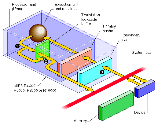
The address of the device is formed in the Execution unit. It may or may not be an address that is mapped by the TLB.
A device address, after mapping if necessary, always falls in one of the ranges that is not cached, so it passes directly to the system bus.
The device or bus attachment recognizes its physical address and responds with data.
The PIO process shown in Figure 1-2 is correct for an SGI Origin 2000 system when the addressed device is attached to the same node. When the device is attached to a different node, the address passes through the connection fabric to that node, and the data returns the same way.
Some devices can perform direct memory access (DMA), in which the device itself, not the CPU, reads or writes data into memory. A device that can perform DMA is called a bus master because it independently generates a sequence of bus accesses without help from the CPU.
In order to read or write a sequence of memory addresses, the bus master has to be told the proper physical address range to use. This is done by storing a bus address and length into the device's registers from the CPU. When the device has the DMA information, it can access memory through the system bus as shown in Figure 1-3.
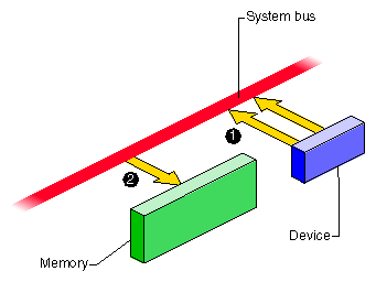
The device places the next physical address, and data, on the system bus.
The memory module stores the data.
In a SGI Origin 2000 system, the device and the memory module can be in different nodes, with address and data passing through the connection fabric between nodes.
When a device is programmed with an invalid physical address, the result is a bus error interrupt. The interrupt is taken by some CPU that is enabled for bus error interrupts. These interrupts are not simple to process for two reasons. First, the CPU that receives the interrupt is not necessarily the CPU from which the DMA operation was programmed. Second, the bus error can occur a long time after the operation was initiated.
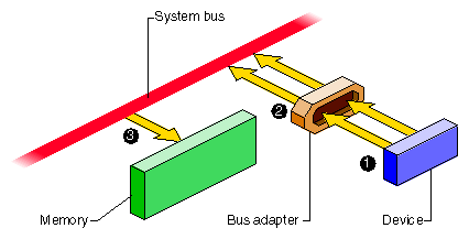
Figure 1-3 is too simple for some devices that are attached through a bus adapter. A bus adapter connects a bus of a different type to the system bus, as shown in Figure 1-4.
For example, the PCI bus adapter connects a PCI bus to the system bus. Multiple PCI devices can be plugged into the PCI bus and use the bus to read and write. The bus adapter translates the PCI bus protocol into the system bus protocol. (For details on the PCI bus adapter, see Part IX, “PCI Drivers”.)
Each bus has address lines that carry the address values used by devices on the bus. These bus addresses are not related to the physical addresses used on the system bus. The issue of bus addressing is made complicated by three facts:
Bus-master devices independently generate memory-read and memory-write commands that are intended to access system memory.
The bus adapter can translate addresses between addresses on the bus it manages, and different addresses on the system bus it uses.
The translation done by the bus adapter can be programmed dynamically, and can change from one I/O operation to another.
This subject can be simplified by dividing it into two distinct subjects: PIO addressing, used by the CPU to access a device, and DMA addressing, used by a bus master to access memory. These addressing modes need to be treated differently.
Programmed I/O (PIO) is the term for a load or store instruction executed by the CPU that names an I/O device as its operand. The CPU places a physical address on the system bus. The bus adapter repeats the read or write command on its bus, but not necessarily using the same address bits as the CPU put on the system bus.
One task of a bus adapter is to translate between the physical addresses used on the system bus and the addressing scheme used within the proprietary bus. The address placed on the target bus is not necessarily the same as the address generated by the CPU. The translation is done differently with different bus adapters and in different system models.
In some older SGI systems, the translation was hard-wired. For a simple example, the address translation from the Indigo2 system bus to the EISA bus was hardwired, so that, for example, CPU access to a physical address of 0x0000 4010 was always translated to location 0x0010 in the I/O address space of EISA slot 4.
With the more sophisticated PCI and VME buses, the translation is dynamic. Both of these buses support bus address spaces that are as large or larger than the physical address space of the system bus. It is impossible to hard-wire a translation of the entire bus address space.
In order to use a dynamic PIO address, a device driver creates a software object called a PIO map that represents that portion of bus address space that contains the device registers the driver uses. When the driver wants to use the PIO map, the kernel dynamically sets up a translation from an unused part of physical address space to the needed part of the bus address space. The driver extracts an address from the PIO map and uses it as the base for accessing the device registers. PIO maps are discussed in Chapter 13, “Services for VME Drivers on Origin 2000/Onyx2”, and in Chapter 20, “PCI Device Attachment”.
A bus-master device on the PCI or VME bus can be programmed to perform transfers to or from memory independently and asynchronously. A bus master is programmed using PIO with a starting bus address and a length. The bus master generates a series of memory-read or memory-write operations to successive addresses. But what bus addresses should it use in order to store into the proper memory addresses?
The bus adapter translates the addresses used on the proprietary bus to corresponding addresses on the system bus. Considering Figure 1-4, the operation of a DMA device is as follows:
The device places a bus address and data on the PCI or VME bus.
The bus adapter translates the address to a meaningful physical address, and places that address and the data on the system bus.
The memory modules stores the data.
The translation of bus virtual to physical addresses is done by the bus adapter and programmed by the kernel. A device driver requests the kernel to set up a dynamic mapping from a designated memory buffer to bus addresses. The map is represented by a software object called a DMA map.
The driver calls kernel functions to establish the range of memory addresses that the bus master device will need to access—typically the address of an I/O buffer. When the driver activates the DMA map, the kernel sets up the bus adapter hardware to translate between some range of bus addresses and the desired range of memory space. The driver extracts from the DMA map the starting bus address, and (using PIO) programs that bus address into the bus master device.
The primary and secondary caches shown in Figure 1-1 are essential to CPU performance. There is an order of magnitude difference in the speed of access between cache memory and main memory. Execution speed remains high only as long as a very high proportion of memory accesses are satisfied from the primary or secondary cache.
The use of caches means that there are often multiple copies of data: a copy in main memory, a copy in the secondary cache (when one is used) and a copy in the primary cache. Moreover, a multiprocessor system has multiple CPU modules like the one shown, and there can be copies of the same data in the cache of each CPU.
The problem of cache coherency is to ensure that all cache copies of data are true reflections of the data in main memory. Different SGI systems use different hardware designs to achieve cache coherency.
In most cases, cache coherence is achieved by the hardware, without any effect on software. In a few cases, specialized software, such as a kernel-level device driver, must take specific steps to maintain cache coherency.
Multiprocessor systems have more complex cache coherency protection because it is possible to have data in multiple caches. In a multiprocessor system, the hardware ensures that cache coherency is maintained under all conditions, including DMA input and output, without action by the software. However, in some systems the cache coherency hardware works correctly only when a DMA buffer is aligned on a cache-line-sized boundary. You ensure this by using the KM_CACHEALIGN flag when allocating buffer space with kmem_alloc() (see “Kernel Memory Allocation” in Chapter 8 and the kmem_alloc(D3) reference page).
In some uniprocessor systems, it is possible for the CPU cache to have newer information than appears in memory. This is a problem only when a bus master device is going to perform DMA. If the bus master reads memory, it can get old data. If it writes memory, the input data can be destroyed when the CPU writes the modified cache line back to memory.
In systems where this is possible, a device driver calls a kernel function to ensure that all cached data has been written to memory prior to DMA output (the dki_dcache_wb(D3) reference page). The device driver calls a kernel function to ensure that the CPU receives the latest data following a DMA input (see the dki_dcache_inval(D3) reference page). In a multiprocessor these functions do nothing, but it is always safe to call them.
The MIPS processors can operate in one of two address modes: 32-bit and 64-bit. The choice of address mode is independent of other features of the instruction set architecture such as the number of available registers and the precision of integer arithmetic. For example, programs compiled to the n32 binary interface use 32-bit addresses but 64-bit integers. The implications for user programs are documented in manuals listed under “Additional Reading”.
The addressing mode can be switched dynamically; for example, the IRIX kernel can operate with 64-bit addresses, but the kernel can switch to 32-bit address when it dispatches a user program that was compiled for that mode. The 32-bit address space is the range of all addresses that can be used when in 32-bit mode. This space is discussed first because it is simpler and more familiar than the 64-bit space.
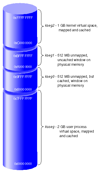
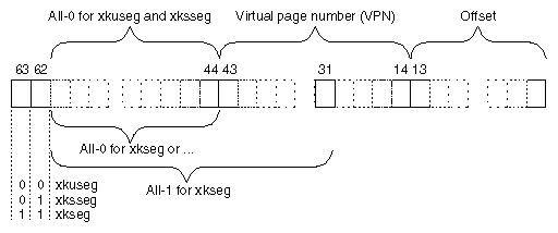
When operating in 32-bit mode, the MIPS architecture uses addresses that are 32-bit unsigned integers from 0x0000 0000 to 0xFFFF FFFF. However, this address space is not uniform. The MIPS hardware divides it into segments, and treats each segment differently. The ranges are shown graphically in Figure 1-5.
The address segments differ in three characteristics:
whether access to an address is mapped; that is, passed through the translation lookaside buffer (TLB)
whether an address can be accessed when the CPU is operating in user mode or in kernel mode
whether access to an address is cached; that is, looked up in the primary and secondary caches before it is sent to main memory
In the mapped segments, each 32-bit address value is treated as shown in Figure 1-6.
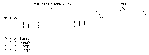
The three most significant bits of the address choose the segment among those drawn in Figure 1-5. When bit 31 is 0, bits 30:12 select a virtual page number (VPN) from 219 possible pages in the address space of the current user process. When bits 31:30 are 11, bits 29:12 select a VPN from 218 possible pages in the kernel virtual address space.
The total 32-bit address space is divided in half. Addresses with a most significant bit of 0 constitute the 2 GB user process space. When executing in user mode, only addresses in kuseg are valid; an attempt to use an address with bit 31=1 causes an addressing exception.
Access to kuseg is always mapped through the TLB. The kernel creates a unique address space for each user process. Of the 219 possible pages in an address space, most are typically unassigned—few processes ever occupy more than a fraction of kuseg—and many are shared pages of program text from dynamic shared objects (DSOs) that are mapped into the address space of every process that needs them.
When bits 31:30 are 11, access is to kernel virtual memory. Only code that is part of the kernel can access this space. References to this space are translated through the TLB. The kernel uses the TLB to map kernel pages in memory as required, possibly in noncontiguous locations. Although pages in kernel space are mapped, they are always associated with real memory. Kernel memory is never paged to secondary storage.
This is the space in which the IRIX kernel allocates such objects as stacks, user page tables, and per-process data that must be accessible on context switches. This area contains automatic variables declared by loadable device drivers. It is the space in which kernel-level device drivers allocate memory. Since kernel space is mapped, addresses in kseg2 that are apparently contiguous need not be contiguous in physical memory. However, a device driver can allocate space that is both logically and physically contiguous, when that is required (see for example the kmem_alloc(D3) reference page).
When address bits 31:29 contain 100, access is directed to physical memory through the cache. If the addressed location is not in the cache, bits 28:0 are placed on the system bus as a physical memory address, and the data presented by memory or a device is returned. Kseg0 contains the exception address to which the MIPS processor branches it when it detects an exception such as an addressing exception or TLB miss.
Since only 29 bits are available for mapping physical memory, only 512 MB of physical memory space can be accessed through this segment in 32-bit mode. Some of this space must be reserved for device addressing. It is possible to gain cached access to wider physical addresses by mapping through the TLB into kseg2, but systems that need access to more physical memory typically run in 64-bit mode (see “Cache-Controlled Physical Memory—xkphys”).
When address bits 31:29 contain 101, access is directly to physical memory, bypassing the cache. Bits 28:0 are placed on the system bus for memory or device transfer.
The kernel refers to kseg1 when performing PIO to devices because loads or stores from device registers should not pass through cache memory. The kernel also uses kseg1 when operating on certain data structures that might be volatile. Kernel-level device drivers sometimes need to write to uncached memory, and must take special precautions when doing so (see “Uncached Memory Access in the IP26 and IP28”).
Portions of kseg0 or kseg1 can be mapped into kuseg by the mmap() function. This is covered at more length under “Memory Use in User-Level Drivers”.
The 64-bit mode is an upward extension of 32-bit mode. All MIPS processors from the R4000 on support 64-bit mode. However, this mode was not used in SGI software until IRIX 6.0 was released.
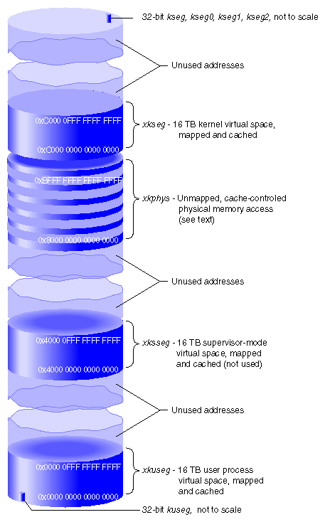
This section refers to the 64-bit address spaces provided by the MIPS R10000 microprocessor. When operating in 64-bit mode, the MIPS architecture uses addresses that are 64-bit unsigned integers from 0x0000 0000 0000 0000 to 0xFFFF FFFF FFFF FFFF. This is an immense span of numbers—if it were drawn to a scale of 1 millimeter per terabyte, the drawing would be 16.8 kilometers long (just over 10 miles).
The MIPS hardware divides the address space into segments based on the most significant bits, and treats each segment differently. The ranges provided by the MIPS R10000 microprocessor are shown graphically in Figure 1-7. These major segments define only a fraction of the 64-bit space. Most of the possible addresses are undefined and cause an addressing exception (segmentation fault) if used.
As in the 32-bit space, these major segments differ in three characteristics:
whether access to an address is mapped; that is, the address is virtual and is passed through the translation lookaside buffer (TLB) to translate the virtual address into a physical address
whether an address can be accessed when the CPU is operating in user mode or in kernel mode
whether access to an address is cached; that is, looked up in the primary and secondary caches before it is sent to main memory
The MIPS-3 instruction set (which is in use when the processor is in 64-bit mode) is designed so that when a 32-bit instruction is used to generate or to load an address, the 32-bit operand is automatically sign-extended to fill the high-order 32 bits.
As a result, any 32-bit address that falls in the user segment kuseg, and which must have a sign bit of 0, is extended to a 64-bit integer with 32 high-order 0 bits. This automatically places the 32-bit kuseg in the bottom of the 64-bit xkuseg, as shown in Figure 1-7.
A 32-bit kernel address, which must have a sign bit of 1, is automatically extended to a 64-bit integer with 32 high-order 1 bits. This places all kernel segments shown in Figure 1-5 at the extreme top of the 64-bit address space. However, these 32-bit kernel spaces are not used by a kernel operating in 64-bit mode.
The two most significant bits of a 64-bit address select the major segments, as shown in Figure 1-7. The xkuseg, xksseg, and xkseg segments access memory using mapped (virtual) addresses and the xkphys segment accesses memory using physical addresses. Virtual and physical addresses use different formats as shown in Figure 1-9 and Figure 1-10.
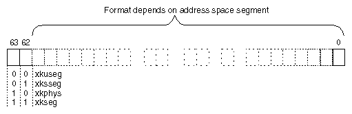
In the mapped segments, each 64-bit virtual address value is formatted as shown in Figure 1-9.
| Note: Some systems that run the MIPS R10000 microprocessors only support virtual address bits 39:0. |
The two most significant bits select the mapped major segment (compare these to the address boundaries in Figure 1-7). For the xkuseg and xksseg segments, bits 61:44 must all be 0. For the xkseg segment, bits 61:44 must all be 0 or bits 61:31 must all be 1, which references the kernel compatibility spaces where the kernel stack is located. (In principle, references to 32-bit kernel segments would have bits 61:40 all 1, but these segments are not used in 64-bit mode.)
The size of a page of virtual memory can vary from system to system and release to release, so always determine it dynamically. In a user-level program, call the getpagesize() function (see the getpagesize(2) reference page). In a kernel-level driver, use the ptob() kernel function (see the ptob(D3) reference page) or the constant NBPP declared in sys/immu.h.
When the page size is 16 KB, bits 13:0 of the address represent the offset within the page, and bits 43:14 select a VPN from the 226, or 64 M, pages in the virtual segment.
The first 16 TB of the address space are devoted to user process space. Access to xkuseg is always mapped through the TLB. The kernel creates a unique address space for each user process. Of the 226 possible pages in a process's address space, most are typically unassigned, and many are shared pages of program text from dynamic shared objects (DSOs) that are mapped into the address space of every process that needs them.
The MIPS architecture permits three modes of operation: user, kernel, and supervisor. When operating in kernel or supervisor mode, the 16 TB space beginning at 0x4000 0000 0000 0000 is accessible. IRIX does not employ the supervisor mode, and does not use xksseg. If xksseg were used, it would be mapped and cached.
When bits 63:62 are 11, access is to kernel virtual memory. Only code that is part of the kernel can access this space, a 16 TB segment starting at 0xC000 0000 0000 0000. References to this space are translated through the TLB, and cached. The kernel uses the TLB to map kernel pages in memory as required, possibly in noncontiguous locations. Although pages in kernel space are mapped, they are always associated with real memory. Kernel pages are never paged to secondary storage.
This is the space in which the IRIX kernel allocates such objects as stacks, per-process data that must be accessible on context switches, and user page tables. This area contains automatic variables declared by loadable device drivers. It is the space in which kernel-level device drivers allocate memory. Since kernel space is mapped, addresses in xkseg that are apparently contiguous need not be contiguous in physical memory. However, a device driver can allocate space that is both logically and physically contiguous, when that is required (see for example the kmem_alloc(D3) reference page).
A 64-bit physical address is formatted as shown in Figure 1-10.
One-quarter of the 64-bit address space—all addresses with bits 63:62 containing 10—are devoted to special access to one or more 1 TB physical address spaces. Any reference to the other spaces (xkuseg and xkseg) is transformed by the TLB into a reference to xkphys. Addresses in this space are interpreted as shown in Figure 1-10.
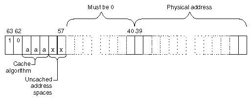
Bits 39:0 select a physical address in a 1 TB range. Bits 57:40 must always contain 0. Bits 61:59 select the hardware cache algorithm to be used. The only values defined for these bits are summarized in Table 1-3.
Table 1-3. Cache Algorithm Selection
Address 61:59 | Algorithm | Meaning |
|---|---|---|
010 | Uncached | This is the 64-bit equivalent of kseg1 in 32-bit mode—uncached access to physical memory. |
110 | Cacheable coherent exclusive on write | This is the 64-bit equivalent of kseg0 in 32-bit mode—cached access to physical memory, coherent access in a multiprocessor. |
011 | Cacheable non-coherent | Data is cached; on a cache miss the processor issues a non-coherent read (one without regard to other CPUs). |
100 | Cacheable coherent exclusive | Data is cached; on a read miss the processor issues a coherent read exclusive. |
101 | Cacheable coherent update on write | Same as 110, but updates memory on a store hit in cache. |
111 | Uncached Accelerated | Same as 010, but the cache hardware is permitted to defer writes to memory until it has collected a larger block, improving write utilization. |
Only the 010 (uncached) and 110 (cached) algorithms are implemented on all systems. The others may or may not be implemented on particular systems.
Bits 58:57 must be 00 unless the cache algorithm is 010 (uncached) or 111(uncached accelerated). Then bits 58:57 can in principle be used to select four other properties to qualify the uncached operation. These bits are first put to use in the SGI Origin 2000 system, described under “Uncached and Special Address Spaces”.
It is not possible for a user process to access either xkphys or xkseg; and not possible for a kernel-level driver to access xkphys directly. Portions of xkphys and xkseg can be mapped to user process space by the mmap() function. This is covered in more detail under “Memory Use in User-Level Drivers”. Portions of xkphys can be accessed by a driver using DMA-mapping and PIO-mapping functions (see “PIO Addresses and DMA Addresses”).
An SGI Origin 2000 system contains one or more nodes. Each node can contain one or two CPUs as well as up to 2 GB of memory. There is a single, flat, address space that contains all memory in all nodes. All memory can be accessed from any CPU. However, a CPU can access memory in its own node in less time than it can access memory in a different node.
The node hardware provides a variety of special-purpose access modes to make kernel programming simpler. These special modes are described here at a high level. For details refer to the hardware manuals listed in “Additional Reading”. These special addressing modes are a feature of the SGI Origin 2000 node hardware, not of the R10000 CPU chip. As such they are available only in the SGI Origin 2000 and Origin200 systems.
Virtual addresses with bits 63:62 containing 00 are references to the user process address space. The kernel creates a virtual address space for each user process as described before (see “Virtual Address Mapping”). The SGI Origin 2000 architecture adds the complication that the location of a page, relative to the location where the process executes, has an effect on the performance of the process. The kernel uses a variety of strategies to locate pages of memory in the same node as the CPU that is running the process.
Kernel virtual addresses (in which bits 63:62 contain 11) are mapped as already described (see “Kernel Virtual Space—xkseg”). Certain important data structures may be replicated into each node for faster access.
The stack and data areas used by device drivers are in xkseg. A driver has the ability to request memory allocation in a particular node, in order to make sure that data about a device is stored in the same node where the device is attached and where device interrupts are taken (see “Kernel Memory Allocation” in Chapter 8).
A physical address in xkphys (bits 63:62 contain 10) has different meanings depending on the settings of bits 61:57 (see Figure 1-10 and Table 1-3). In the SGI Origin 2000 architecture, these bits are interpreted by the memory control circuits of the node, external to the CPU. The possibilities are listed in Table 1-4. Some are covered in more detail in following topics.
Table 1-4. Special Address Spaces in SGI Origin 2000
Address 61:59 (Algorithm) |
|
|
|---|---|---|
110 (cached) | n.a. | Cached access to physical memory |
010 (uncached) | 00 | Node special memory areas including directory cache, ECC, PROM, and other node hardware locations. |
010 (uncached) | 01 | I/O space: addresses that can be mapped into the address space of any bus adapter. |
010 (uncached) | 10 | Synchronization access to memory. |
010 (uncached) | 11 | Uncached access to physical memory. |
When the CPU emits a translated virtual address with bits 63:62 containing 10 and bits 61:59 specifying cached access, the address is a cached reference to physical memory. When the referenced location is not contained in the secondary cache, it is fetched from memory in the node that contains it. This is the normal outcome of the translation of a user or kernel virtual address through the TLB.
The actual address is the physical address in bits 39:0, interpreted as shown in Figure 1-11.
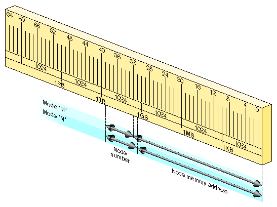
The node hardware can operate in either of two modes, called `M' and `N'.
| Mode `M' | |
Bits 39:32 select one of 256 nodes. Remaining bits select an address in as much as 4 GB of memory in that node. | |
| Mode `N' | |
Bits 39:31 select one of 512 nodes. Remaining bits select an address in as much as 2 GB of memory in that node. | |
Either mode places the memory that is part of each node in a flat address space with a potential size of 1 TB. All locations are accessed in the same way—there is a single address space for the entire system. For example, the memory that is part of node 1 begins at 0x0000 0001 0000 0000 (in mode `M') or 0x0000 0000 8000 0000 (in mode `N').
The node hardware implements one special case: addresses in the range 0-63 MB (0 through 0x0000 0000 03ff ffff) are always treated as a reference to the current node. In effect, the current node number is logically ORed with the address. This allows trap handlers and other special code to refer to node-specific data without having to know the number of the node in which they execute.
A physical address in xkphys (bits 63:62 contain 10) that has the uncached algorithm (bits 61:59 contain 010) always bypasses the secondary cache. An address of this form can access physical memory in either of two ways.
When bits 58:57 contain 11, the address bits 39:0 are decoded as shown in Figure 1-11. In this mode there is no aliasing of addresses in the range 0-63 MB to the current node; the node number must be given explicitly.
However, when bits 58:57 contain 00, an address in the range 0-768 MB is interpreted as uncached access to the memory in the current node. In effect, the node number is ORed into the address. Also in this mode, access to the lowest 64 KB is swapped between the two CPUs in a node. CPU 0 access to addresses 0x0 0000 through 0x1 ffff is directed to those addresses. But CPU 1 access to 0x0 0000 goes to 0x1 0000, and access to 0x1 0000 goes to 0x0 0000—reversing the use of the first two 64 KB blocks. This helps trap handlers that need quick access to a 64 KB space that is unique to the CPU.
An uncached physical address with bits 58:57 containing 10 is an atomic fetch-and-modify access. Bits 39:6 select a memory unit of 64 bytes (half a cache line) and bits 5:3 select an operation, as shown in Figure 1-12.
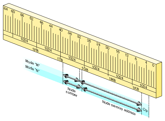
The first word or doubleword (depending on the instruction being executed) of the addressed unit is treated as shown in Table 1-5.
Table 1-5. SGI Origin 2000 Fetch-and-Op Operations
Instruction | Address 5:3 | Operation |
|---|---|---|
Load | 000 | An uncached read of the location. |
Load | 001 | Fetch-and-increment: the old value is fetched and the memory value is incremented. |
Load | 010 | Fetch-and-decrement: the old value is fetched and the memory value is decremented. |
Load | 011 | Fetch-and-zero: the old value is returned and zero is stored. |
Store | 000 | An uncached store of the location. |
Store | 001 | Increment: the memory location is incremented. |
Store | 010 | Decrement: the memory location is decremented. |
Store | 011 | AND: memory data is ANDed with the store data. |
Store | 100 | OR: memory data is ORed with the store data. |
These are atomic operations; that is, no other CPU can perform an interleaved operation to the same 64-byte unit. The kernel can use this addressing mode to implement locks and other synchronization operations. A user-level library is also available so that normal programs can use these facilities when they are available; see the fetchop(3) reference page.
Memory use by device drivers is simpler than the details in this chapter suggest. The primary complication for the designer is the use of 64-bit addresses, which may be unfamiliar.
You must take account of a number of considerations when porting an existing C program to an environment where 64-bit mode is used, or might be used. This can be an issue for all types of drivers, kernel-level and user-level alike. For detailed discussion, see the MIPSpro 64-Bit Porting and Transition Guide listed in “Additional Reading”.
The most common problems arise because the size of a pointer and of a long integer changes between a program compiled with the -64 option and one compiled -32. When you use pointers, longs, or types derived from longs, in structures, the field offsets differ between the two modes.
When all programs in the system are compiled to the same mode, there is no problem. This is the case for a system in which the kernel is compiled to 32-bit mode: only 32-bit user programs are supported. However, a kernel compiled to 64-bit mode executes user programs in 32-bit or 64-bit mode. A structure prepared by a 32-bit program—a structure passed as an argument to ioctl(), for example—does not have fields at the offsets expected by a 64-bit kernel device driver. For more on this specific problem, see “Handling 32-Bit and 64-Bit Execution Models” in Chapter 7.
The basic strategy to make your code portable between 32-bit and 64-bit kernels is to be extremely specific when declaring the types of data. You should almost never declare a simple “int” or “char.” Instead, use a data type that is explicit as to the precision and the sign of the variable. The header files sgidefs.h and sys/types.h define type names that you can use to declare structures that always have the same size. The type __psint_t, for example, is an integer the same size as a pointer; you can use it safely as alias for a pointer. Similarly, the type __uint32_t is guaranteed to be an unsigned, 32-bit, integer in all cases.
When you control a device from a user process, your code executes entirely in user process space, and has no direct access to any of the other spaces described in this chapter.
Depending on the device and other considerations, you may use the mmap() function to map device registers into the address space of your process (see the mmap(2) reference page). When the kernel maps a device address into process space, it does it using the TLB mechanism. From mmap() you receive a valid address in process space. This address is mapped through a TLB entry to an address in segment that accesses uncached physical memory. When your program refers to this address, the reference is directed to the system bus and the device.
Portions of kernel virtual memory (kseg0 or xkseg) can be accessed from a user process. Access is based on the use of device special files (see the mem(7) reference page). Access is done using two models, a device model and a memory map model.
The device special file /dev/mem represents physical memory. A process that can open this device can use lseek() and read() to copy physical memory into process virtual memory. If the process can open the device for output, it can use write() to patch physical memory.
The device special file /dev/kmem represents kernel virtual memory (kseg0 or xkseg). It can be opened, read and written similarly to /dev/mem. Clearly both of these devices should have file permissions that restrict their use even for input.
The mmap() function allows a user process to map an open file into the process address space (see the mmap(2) reference page). When the file that is mapped is /dev/mem, the process can map a specified segment of physical memory. The effect of mmap() is to set up a page table entry and TLB entry so that access to a range of virtual addresses in user space is redirected to the mapped physical addresses in cached physical memory (kseg0 or the equivalent segment of xkphys).
The /dev/kmem device, representing kernel virtual memory, cannot be used with mmap(). However, a third device special, /dev/mmem (note the double “m”), represents access to only those addresses that are configured in the file /var/sysgen/master.d/mem. As distributed, this file is configured to allow access to the free-running timer device and, in some systems, to graphics hardware.
For an example of mapped access to physical memory, see the example code in the syssgi(2) reference page related to the SGI_QUERY_CYCLECNTR option. In this operation, the address of the timer (a device register) is mapped into the process's address space using a TLB entry. When the user process accesses the mapped address, the TLB entry converts it to an address in kseg1/xkphys, which then bypasses the cache.
A kernel-level device driver can provide mapped access to device registers or to memory allocated in kernel virtual space. An example of such a driver is shown in Part III, “Kernel-Level Drivers”.
When you control a device from a kernel-level driver, your code executes in kernel virtual space. The allocation of memory for program text, local (stack) variables, and static global variables is handled automatically by the kernel. Besides designing data structures so they have a consistent size, you have to consider these special cases:
dynamic memory allocation for data and for buffers
transferring data between kernel space and user process space
getting addresses of device registers to use for PIO
The kernel supplies utility functions to help you deal with each of these issues, all of which are discussed in Chapter 8, “Device Driver/Kernel Interface”.
Access to uncached memory is not supported in these systems, in which cache coherency is maintained by the hardware, even under access from CPUs and concurrent DMA. There is never a need (and no approved way) to access uncached memory in these systems.
The IP26 CPU module is used in the SGI Power Indigo2 workstation and the Power Challenge M workstation. Both are deskside workstations using the R8000 processor chip. These remarks also apply to the IP28 CPU used in the Power Indigo2 R10000 workstation. In these machines, extra care must be taken in cache management.
When an I/O device is going to perform DMA input to memory, the device driver must invalidate any cached copies of the buffer that will receive the data. If this is not done, the CPU could go on using the “stale” data in the cache, ignoring the input data placed in memory by the device. This is done by calling the dki_dcache_inval() function to invalidate the range of addresses where DMA input is planned.
In the IP28 CPU, the delayed and speculative execution features of the R10000 processor make it necessary for the driver to invalidate the cache twice: once before initiating the DMA input, and once again immediately after DMA ends.
Before initiating DMA output, the driver must force all cached data to memory by calling dki_dcache_wb(). This ensures that recent data in the cache is also present in memory before the device begins to access memory. The use of both these functions is discussed further under “Managing Memory for Cache Coherency” in Chapter 8.
Cache invalidation is handled automatically when you use the userdma() and undma() functions to lock memory for DMA (see “Setting Up a DMA Transfer” in Chapter 8).
The Indigo2 systems use ECC memory (error-correcting code memory, which can correct for single-bit errors on the fly). ECC memory is also used in large multiprocessor systems from SGI, where it has no effect on performance.
In the IP26 and IP28, although ECC memory has no impact on the performance of normal, cached memory access, uncached access can be permitted only when the CPU is placed in a special, “slow” access mode.
A device driver may occasionally need to write directly to uncached memory (although it is better to write to cached memory and then use dki_dcache_wb()). Before doing so, the driver must put the CPU in “slow” mode by calling the function ip26_enable_ucmem(). As soon as the uncached store is complete, return the system to “fast” mode by calling ip26_return_ucmem(). (See the ip26_ucmem(D3) reference page.) While the CPU is in “slow” mode, several clock cycles are added to every memory access, so do not keep it in “slow” mode any longer than necessary.
These functions can be called in any system. They do nothing unless the CPU is an IP26 or IP28.