The Peripheral Component Interconnect (PCI) bus, initially designed at Intel Corp, is standardized by the PCI Bus Interest Group, a nonprofit consortium of vendors (see “Standards Documents” and “Internet Resources”).
The PCI bus is designed as a high-performance local bus to connect peripherals to memory and a microprocessor. In many personal computers based on Intel and Motorola processors, the PCI bus is the primary system bus. A wide range of vendors make devices that plug into the PCI bus.
The PCI bus is supported by the O2 and Octane workstations, by the Origin 2000 architecture, and by the Origin 200 deskside systems. This chapter contains the following topics related to support for the PCI bus:
“PCI Bus in SGI Workstations” gives an overview of PCI bus features and implementation.
“PCI Implementation in O2 Workstations” describes the hardware features and restrictions of the PCI bus in low-end workstations.
“PCI Implementation in Origin Servers” describes the features of the PCI implementation in larger architectures.
More information about PCI device control appears in these chapters:
Chapter 4, “User-Level Access to Devices”, covers PIO and DMA access from the user process.
Chapter 21, “Services for PCI Drivers”, discusses the kernel services used by a kernel-level VME device driver, and contains an example.
This section contains an overview of the main features of PCI hardware attachment, for use as background material for software designers. Hardware designers can obtain a detailed technical paper on PCI hardware through the SGI Developer Program (it appears in the Developer Toolbox CDROM, and is also available separately). That paper covers important design issues such as card dimensions, device latencies, power supply capacities, interrupt line wiring, and bus arbitration.
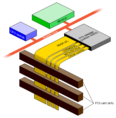
In no IRIX system is the PCI bus the primary system bus. The primary system bus is always a proprietary bus that connects one or more CPUs with high-performance graphics adapters and main memory: The PCI bus adapter is connected (or “bridged,” in PCI terminology) to the system bus, as shown in Figure 20-1.
In the O2 workstation, the primary system bus is a high-bandwidth connection between the CPU, memory, and the display hardware (whose bandwidth requirements are almost as high as the CPU's).
In the Octane workstation, the PCI bus adapter is bridged to the XIO bus adapter, which is in turn a client of the system crossbar for access to the CPU or memory.
In the Origin series, the PCI bus adapter is bridged to the XIO bus adapter, which in turn connects to a Hub chip for access to memory in the local module and to the Cray interconnection fabric for access to memory in other modules.
Different SGI systems have different PCI adapter ASICs. Although all adapters conform to the PCI standard level 2.1, there are significant differences between them in capacities, in optional features such as support for the 64-bit extension, and in performance details such as memory-access latencies.
The PCI adapter is a custom circuit with these main functions:
To act as a PCI bus target when a PCI bus master requests a read or write to memory
To act as a PCI bus master when a CPU requests a PIO operation
To manage PCI bus arbitration, allocating bus use to devices as they request it
To interface PCI interrupt signals to the system bus and the CPU
A system may contain one or more PCI bus adapters. Each bus connects one or more physical packages. The PCI standard allows up to 32 physical packages on a bus. A “package” may consist of a card plugged into a slot on the bus. However, a “package” can also consist of an internal chipset mounted directly on the system board, using the PCI bus and occupying one or more virtual slots on the bus. For example, the SCSI adapter in the O2 workstation occupies the first two virtual slots of the PCI bus in that system.
Each physical package can implement from one to eight functions. A PCI function is an independent device with its own configuration registers in PCI configuration space, and its own address decoders.
In SGI systems, each PCI function is integrated into IRIX as a device. A PCI device driver manages one or more devices in this sense. A driver does not manage a particular package, or card, or bus slot; it manages one or more logical devices.
| Note: IRIX 6.3 for the O2 workstation supports multifunction cards. However, IRIX 6.4 for Origin, Onyx2, and Octane does not support multifunction cards. Support for multifunction cards returns for all hardware platforms with IRIX 6.5. |
All SGI PCI implementations permit peer-to-peer transactions, in which two PCI devices exchange data without the involvement of the bus adapter except as arbitrator. However, most PCI transactions take place between a PCI device and system memory, by way of the bus adapter.
Two important facts about PCI-to-memory transaction are, first, that memory is not located on the PCI bus and in fact, the PCI bus competes for the use of memory with the CPU and other devices on the system bus; and second, that memory in SGI systems is organized around cache lines of 128 bytes. When a PCI device initiates a read to memory, the bus adapter requests a cache line from memory, and returns the addressed word from that line. When a PCI device initiates a write to memory, the bus adapter fetches the addressed line; stores successive words into it until the operation ends or another line is addressed; and writes the line back to memory.
Some important implications follow:
The latency of access to the first byte or word in a cache line can be long—in the range of multiple microseconds, if the system bus is heavily used.
Access to subsequent words in the same cache line can go at maximum bus speed.
A PCI bus master that attempts to read small fields scattered in memory will be constrained to run at the rate at which the PCI adapter can fetch entire cache lines from memory. A PCI bus master that attempts to write small fields scattered in memory will be constrained even further, to the rate at which the PCI adapter can perform read-modify-write cycles of entire cache lines.
A device that performs streaming access to consecutive locations can operate at good speed, once the initial latency period is past. However, a streaming device must have enough on-card buffer capacity to hold data during the maximum latency.
These issues of latency are discussed in much greater detail in a document available from the SGI developer support organization.
The order of bytes in a word, also called “endianness,” is in conflict between PCI devices and MIPS-based software. MIPS-based software is “big-endian,” placing the most significant byte (MSB) of a 32-bit word at the lowest (“leftmost”) address. Devices made for the PCI bus typically use “little-endian,” or Intel, byte ordering, in which the MSB is at the highest address. Whether the bus hardware should perform byte-swapping to compensate is a difficult question with no universal answer. The question is complicated by the facts that in some systems, PCI data passes through more than one bus adapter between the device and memory, and the default settings of the byte-swapping hardware is different between different SGI platforms.
When considering byte order, consider the intended use of the data (user data or driver command/status), and the method (PIO or DMA, which use different hardware).
When considering only a stream of bytes being transferred between memory and some kind of storage medium—for example, a block of data being read or written from a tape—the byte order of the device is not significant. The system writes the stream; later the system reads the stream back. As long as the bus treats the data the same way on input as on output, the data returns to memory in the same order it had when it left.
What you want to ensure is that, if the storage medium is transferred to a PCI device on another machine, the same sequence of bytes will arrive in the other machine's memory. This is the best you can do toward compatibility between big-endian and little-endian programs—preserving memory byte order. Interpretation of binary items embedded within the byte stream is a problem for the software.
When considering data that is interpreted by the device driver and by the PCI device—for example, the contents of a device status register, or words giving the address and length of a DMA transfer—byte order does matter. You must know if your device uses little-endian binary integers, and you must ensure that an integer (count or address) is byte-swapped, if necessary, on the way to the device so it can be interpreted correctly.
PCI adapters are set up so that when a driver does 32-bit PIO to 32-bit boundaries, a 32-bit count or address is translated correctly between big-endian and little-endian forms, as shown in Table 20-1.
Table 20-1. PIO Byte Order in 32-bit Transfer
Byte On System Bus | IRIX Use | Byte on PCI Bus |
|---|---|---|
0 | MSB | 3 |
1 |
| 2 |
2 |
| 1 |
3 | LSB | 0 |
PCI configuration space is accessed using PIO. You can declare a memory copy of configuration space as shown in Example 20-1.
Example 20-1. Declaration of Memory Copy of Configuration Space
typedef struct configData_s { /* based on PCI standard */
   unsigned short vendorID, deviceID; /* order reversed */
   unsigned short command, status;    /* order reversed */
   unsigned char revID, prog_if, subclase,class; /* reversed */
   unsigned char cacheSize, latency, hdrType, BIST;/* reversed */
   __uint32_t BAR[6];
   __uint32_t cardbus;
   unsigned short subvendorID, subsystemID; /* reversed */
   __uint32_t eromBAR;
   __uint32_t reserved[2];
   unsigned char intLine, intPin, maxGrant, maxLat; /* reversed */
} configData_t;

typedef union configCopy_u { /* union with word array */
   __uint32_t word[16];
   configData_t cfg;
} configCopy_t;
|
The device driver loads the memory copy by getting 32-bit words using PIO and storing them into the union fields word. In the course of each word-copy, byte order is reversed, which preserves the significance value of 32-bit and 16-bit words, but reverses the order of 16-bit and 8-bit subfields within words. The copied data can be accessed from the configData_t structure in the union.
The same approach applies to PIO to the PCI bus memory and I/O address spaces—use 32-bit transfers on 32-bit boundaries for correct logical results on data of 32 bits and less. Alternatively, to perform PIO to a 16-bit or 8-bit unit, take the address from the PIO map and exclusive-OR it with 0x03 to produce the byte-swapped address of the unit.
PIO can be done in 64-bit units as well as 32-bit units. In this case, each 32-bit unit is treated separately. The most-significant 32-bit half of the value is sent first, and is stored in the lower PCI address. Unfortunately this is not what a PCI device expects in, for example, a 64-bit Base Address Register (BAR). In order to store 64-bit addresses in a PCI register, do one of the following:
Reverse the order of 32-bit halves in the CPU before storing the 64-bit value.
Store the 32-bit halves separately, the less-significant half first.
The same problem occurs on input of a 64-bit quantity to a long long value: the less-significant word appears in the more-significant half of the received variable.
A driver prepares for DMA access by creating a DMA map (see “Using DMA Maps” in Chapter 21). When a map is allocated, you specify one of two flags: PCI_BYTE_STREAM or PCI_WORD_VALUES. All transfers through the map are appropriate for either a data stream or a command stream, as requested.
In the O2 workstation, a proprietary system bus connects the CPU, multimedia devices (audio, video, and graphics) and main memory. Multimedia use is a central focus of this workstation's design, and audio and video devices have highest priority, after the CPU, for bandwidth on the system bus.
The PCI bus adapter interfaces one PCI bus to this system bus. The PCI bus adapter is a unit on the system bus, on a par with other devices. The PCI bus adapter competes with the CPU and with multimedia I/O for the use of main memory.
The built-in SCSI adapter, which is located on the main system board, is logically connected to the PCI bus and takes the place of the first two “slots” on the PCI bus, so that the first actual slot is number 2.
In the O2, the PCI adapter implements a standard, 32-bit PCI bus operating at 33 MHZ. The following optional signal lines are not supported.
The LOCK# signal is ignored; atomic access to memory is not supported.
The cache-snoop signals SBO# and SDONE are ignored. Cache coherency must be ensured by the driver.
The JTAG signals are not supported.
When the IRIX kernel probes the PCI bus and finds an active device, it initializes the device configuration registers as follows:
Command Register | The enabling bits for I/O Access, Memory Access, and Master are set to 1. Other bits, such as Memory Write and Invalidate and Fast Back-to-Back are left at 0. |
Cache Line Size | 0x20 (32, 32-bit words, or 128 bytes). |
Latency Timer | 0x30 (48 clocks, 1.45 microseconds). |
Base Address registers | Each register that requests memory or I/O address space is programmed with a starting address. In the O2 system, memory addresses are always greater than 0x8000 0000. |
The device driver may set any other configuration parameters when attaching a device.
| Caution: If the driver changes the contents of a Base Address Register, the results are unpredictable. Don't do this. |
The relationship between the PCI bus address space and the system memory physical address space differs from one system type to another.
The O2 PCI adapter supports 64-bit data transfers, but not 64-bit addressing. All bus addresses are 32 bits, that is, all PCI bus virtual addresses are in the 4 GB range. The Dual Address Cycle (DAC) command is not supported (or needed).
The 64-bit extension signals AD[63:32], C/BE#[7:4], REQ64# and ACK64# are pulled up as required by the PCI standard.
When the PCI bus adapter operates as a bus master (as it does when implementing a PIO load or store for the CPU), the PCI adapter generates 32-bit data cycles.
When the PCI bus adapter operates as a bus target (as it does when a PCI bus master transfers data using DMA), the PCI adapter does not respond to REQ64#, and hence 64-bit data transfers are accomplished in two, 32-bit, data phases as described in the PCI specification.
For PIO purposes (CPU load and store access to a device), memory space defined by each PCI device in its configuration registers is allocated in the upper two gigabytes of the PCI address space, above 0x8000 0000. These addresses are allocated dynamically, based on the contents of the configuration registers of active devices. The I/O address space requested by each PCI device in its configuration registers is also allocated dynamically as the system comes up. Device drivers get a virtual address to use for PIO to any address space by creating a PIO map (see “Using PIO Maps” in Chapter 21).
It is possible for a PCI device to request (in the initial state of its Base Address Registers) that its address space be allocated in the first 1 MB of the PCI bus. This request cannot be honored in the O2 workstation. Devices that cannot decode bus addresses above 0x8000 0000 are not supported.
PIO access to configuration space is supported. However, drivers must not only create a PIO map, but must use kernel functions instead of simply loading and storing to a translated address.
The O2 workstation supports a 1 GB physical memory address space (30 bits of physical address used). Any part of physical address space can be mapped into PCI bus address space for purposes of DMA access from a PCI bus master device. The device driver ensures correct mapping through the use of a DMA map object (see “Using DMA Maps” in Chapter 21).
Two devices that are built into the workstation take the positions of PCI bus slots 0 and 1. Actual bus slots begin with slot 2 and go up to a maximum of slot 4 (the built-in devices and a design maximum of three physical slots).
The PCI adapter maintains two priority groups. The lower-priority group is arbitrated in round-robin style. The higher-priority group uses fixed priorities based on slot number, with the higher-numbered slot having the higher fixed priority.
The IRIX kernel assigns slots to priority groups dynamically by storing values in an adapter register. There is no kernel interface for changing this priority assignment. The audio and the available PCI slots are in the higher priority group.
The PCI adapter can present eight unique interrupt signals to the system CPU. The IRIX kernel uses these interrupt signals to distinguish between the sources of PCI bus interrupts. The system interrupt numbers 0 through 7 are distributed across the PCI bus slots as shown in Table 20-2.
Table 20-2. PCI Interrupt Distribution to System Interrupt Numbers
PCI Interrupt | Slot 0 (built-in device) | Slot 1(built-in device) |
| Slot 3 | Slot 4 |
|---|---|---|---|---|---|
INTA# | system 0 | n.c. | system 2 | system 3 | system 4 |
INTB# | n.c. | system 1 | system 5 | system 7 | system 6 |
INTC# | n.c. | n.c. | system 6 | system 5 | system 7 |
INTD# | n.c. | n.c. | system 7 | system 6 | system 5 |
Each physical PCI slot has a unique system interrupt number for its INTA# signal. The INTB#, INTC#, and INTD# signals are connected in a spiral pattern to three system interrupt numbers.
In the Origin 2000, Onyx2, and Origin 200 systems, the PCI adapter bridges to the XIO bus, a high-speed I/O bus. This joins the PCI bus into the connection fabric, so any PCI bus can be addressed from any module, and any PCI bus can access memory that is physically located in any module. In the Octane workstation, the same PCI adapter ASIC is used to bridge the PCI bus to a proprietary system bus.
In these systems the multimedia features have substantial local resources, so that contention with multimedia for the use of main memory is lower than in the O2 workstation. However, these systems also have multiple CPUs and multiple layers of address translation, and these factors can introduce latencies in PCI transactions.
It is important to understand that there is no guaranteed order of execution between separate PCI transactions in these systems. There can be multiple hardware layers between the CPU, memory, and the device. One or more data transactions can be “in flight” for durations that are significant. For example, suppose that a PCI bus master device completes the last transfer of a DMA write of data to memory, and then executes a DMA write to update a status flag elsewhere in memory.
Under circumstances that are unusual but not impossible, the status in memory can be updated, and acted upon by software, while the data transaction is still “in flight” and has not completely arrived in memory. The same can be true of a PIO read that polls the device—it can return “complete” status from the device while data sent by DMA has yet to reach memory.
Ordering is guaranteed when interrupts are used. An interrupt handler is not executed until all writes initiated by the interrupting device have completed.
When the IRIX 6.5 kernel probes the PCI bus and finds an active device, it initializes the device configuration registers as follows:
Command Register | The enabling bits for I/O Access, Memory Access, and Master are set to 1. Other bits, such as Memory Write and Invalidate and Fast Back-to-Back are left at 0. |
Cache Line Size | 0x20 (32, 32-bit words, or 128 bytes). |
Latency Timer | 0x30 (48 clocks, or 1.45 us). |
Base Address registers | Each register that requests memory or I/O address space is programmed with a starting address. Under IRIX 6.5, memory space addresses are below 0x4000 0000. |
The device driver may set any other configuration parameters when attaching a device.
| Caution: If the driver changes the contents of a Base Address Register, the results are unpredictable. Don't do this. |
In these larger systems, the PCI adapter implements a standard, 64-bit PCI bus operating at 33 MHZ. The following optional signal lines are not supported.
The LOCK# signal is ignored; atomic access to memory is not supported.
The cache-snoop signals SBO# and SDONE are ignored. Cache coherency is ensured by the PCI adapter and the memory architecture, with assistance by the driver.
In these systems, addresses are translated not once but at least twice and sometimes more often between the CPU and the device, or between the device and memory. Also, some of the logic for features such as prefetching and byte-swapping is controlled by the use of high-order address bits. There is no simple function on a physical memory address that yields a PCI bus address (nor vice-versa). It is essential that device driver use PIO and DMA maps (see Chapter 21, “Services for PCI Drivers”).
These systems support 64-bit data transactions. Use of 64-bit data transactions results in best performance.
The PCI adapter accepts 64-bit addresses produced by a bus master device. The PCI adapter does not generate 64-bit addresses itself (because the PCI adapter generates addresses only to implement PIO transactions, and PIO targets are always located in 32-bit addresses).
For PIO purposes, memory space defined by each PCI device in its configuration registers is allocated in the lowest gigabyte of PCI address space, below 0x400 0000. These addresses are allocated dynamically, based on the contents of the configuration registers of active devices. The I/O address space requested by each PCI device in its configuration registers is also allocated dynamically as the system comes up. A driver can request additional PCI I/O or Memory space when the device uses space beyond that described by its configuration registers.
Device drivers get a virtual address to use for PIO in any address space by creating a PIO map (see “Using PIO Maps” in Chapter 21).
It is possible for a PCI device to request (in the initial state of its Base Address Registers) that its address space be allocated in the first 1 MB of the PCI bus. This request is honored in larger systems (it cannot be honored in the O2 workstation, as noted under “PCI Implementation in O2 Workstations”).
PIO access to configuration space is supported. However, drivers use kernel functions instead of simply loading and storing to a translated address.
Any part of physical address space can be mapped into PCI bus address space for purposes of DMA access from a PCI bus master device. As described under “Address Space Usage in SGI Origin 2000 Systems” in Chapter 1, the Origin 2000 architecture uses a 40-bit physical address, of which some bits designate a node board. The PCI adapter sets up a translation between an address in PCI memory space and a physical address, which can refer to a different node from the one to which the PCI bus is attached.
The device driver ensures correct mapping through the use of a DMA map object (see “Using DMA Maps” in Chapter 21).
If the PCI device supports only 32-bit addresses, DMA addresses can be established in 32-bit PCI space. When this requested, extra mapping hardware is used to map a window of 32-bit space into the 40-bit memory space. These mapping registers are limited in number, so it is possible that a request for DMA translation could fail. For this reason it is preferable to use 64-bit DMA mapping when the device supports it.
When the device supports 64-bit PCI bus addresses for DMA, the PCI adapter can use a simpler mapping method from a 64-bit address into the target 40-bit address, and there is less chance of contention for mapping hardware. The device driver must request a 64-bit DMA map, and must program the device with 64-bit values.
The PCI adapter maintains two priority groups, the real-time group and the low-priority group. Both groups are arbitrated in round-robin style. Devices in the real-time group always have priority for use of the bus. There is no kernel interface for changing the priority of a device.
There are two unique interrupt signals on each PCI bus. The INTA# and INTC# signals are wired together, and the INTB# and INTD# signals are wired together. A PCI device that uses two distinct signals must use INTA and INTB, or INTC and INTD. A device that needs more than two signals can use the additional signal lines, but such a device must also provide a register from which the device driver can learn the cause of the interrupt.
The bridge chip that is used on all Octane and Origin systems (which includes the SGI 3000 server series) has eight input interrupts. PCI cards , however, can implement up to four different interrupts (A, B, C, and D), which may create a shared condition. Table 20-3 shows how interrupts can be shared on an Origin system.
Table 20-3. PCI Card Interrupt Pin Distribution
PCI slots | PCI Interrupt line A | PCI interrupt line B | PCI interrupt line C | PCI interrupt line D |
|---|---|---|---|---|
Slot 0 | 0 | 4 | 0 | 4 |
Slot 1 | 1 | 5 | 1 | 5 |
Slot 2 | 2 | 6 | 2 | 6 |
Slot 3 | 3 | 7 | 3 | 7 |
Slot 4 | 4 | 0 | 4 | 0 |
Slot 5 | 5 | 1 | 5 | 1 |
Slot 6 | 6 | 2 | 6 | 2 |
Slot 7 | 7 | 3 | 7 | 3 |
For example, if a card in slot 0 uses INTA# and a card in slot 4 uses INTB#, there will be a conflict. In this case, the interrupt service routines (ISRs) of both cards will be called when the bridge interrupt pin 0 transitions to active. If you try to connect to all four interrupt lines from the card, you will create a shared condition. The interrupts that are shared cannot be redirected with the DEVICE_ADMIN statements in the /var/sysgen/system/irix.sm file.