This appendix details hardware specifications for Sirius Video:
compatibility
CP interface
VME interface
analog input and output channel specifications
video formats
host connector specifications
Sirius Video breakout box connectors
Sirius Video connectors and controls
Sirius Video is compatible with the NTSC and PAL television standards. It is also compatible with CCIR 601 and SMPTE 125M digital video standards.
CP interface bandwidth is 40 MHz, at up to 48 bits wide. You can choose between 8 and 10 bits per component.
The VME interface on the Sirius Video board initializes and configures the hardware and, in master mode, transfers video to and from system memory. A Sirius Video application can send live video to raster or texture memory in the graphics subsystem, or it can send the video to host memory over the VME bus. Regardless of input format, the video stream within Sirius Video is 4:4:4:4 RGBa/YUVa, 10 bits per component.
With the exception of video frame buffers, all other Sirius Video board devices can be accessed by programmed I/O (PIO) cycles. Supported VME PIOs are A16, D32, read and write, nonprivileged access; address modifier is 0x29. Except for the VME controller registers, any Sirius Video board device can be accessed using the DMA transfer (read or write) cycle.
Four different interrupt levels are supported; the four upper bits of the status and ID registers are software-programmable.
In its default slave mode, the VME interface initializes and configures the Sirius Video hardware.
The interface can be programmed to select VME master mode, perform 32-bit (D32) or 64-bit (D64) DMA transfers to or from host memory over the VME bus, and return to VME slave mode. The VME master can be programmed to give up the bus when other VME masters request it (Release On Request) and finish its assigned tasks later when the bus is available again, or to hold onto the bus until its tasks are finished (Release When Done).
For multiple-pixel transfers, Sirius Video supports pixel packing and unpacking. Transfer rate is ~28 MB/second for 32-bit transfers and
~55 MB/second for 64-bit transfers. D64 mode is available only on Sirius Video installed in Onyx and CHALLENGE systems.
The VME interface includes VLISTs, which are FIFOs implemented in local memory on the Sirius Video board. The host can put commands for managing the state of the Sirius Video board into the VLISTs, thus freeing the host from having to manage the Sirius Video board state directly during vertical blanking.
Because a dedicated hardware controller performs the writes during vertical blanking, greater data rates are possible than if the host performed this task directly over the VME bus. VLIST commands are in the form of writes to Sirius Video board resources, such as command registers and lookup tables.
Table A-1 lists some general technical specifications for analog input and output channels. and genlock jitter.
Table A-1. Analog Input and Output Channel Specs
Specification | Channel | Value |
|---|---|---|
Input impedance | Input | 50 KOhm; 5 pF capacitance |
Frequency response | Input Output | +/- 0.25 dB to 1 MHz; +/- 0.5 dB to 5.4 MHz +/- 0.25 dB to 1 MHz; +/- 0.5 dB to 5.2 MHz with sin X/X compensation |
Group delay | Both types | +/- 20 nsec to 5.5 MHz |
Return loss | Input | >40 dB to 5.5 MHz |
Analog S/N ratio | Input | >55 dB, unweighted 5.0 MHz (GBR or YUV) |
Analog S/N ratio | Output | >63 dB, typical unweighted 5.0 MHz (GBR or YUV) |
Line-locked genlock sync jitter | Output genlock | <10 nsec |
Frequency response, transient response, signal-to-noise (S/N) ratio, and crosstalk are all included for both input and output sections, including the breakout box. The measurements were made with a Tektronix model 2465A (with TV trigger) oscilloscope and a Tektronix VM700A video measurement set. Analog test signals were generated by Tektronix generator models TSG-130A, TSG-131A, and TSG-100; and digital test signals were generated by Tektronix generator model TSG-422.
This section discusses analog input and output measurements separately.
This section discusses
frequency response
transient (K-factor) response
signal-to-noise ratio
input genlock jitter
input genlock signal-to-noise ratio and crosstalk
composite input
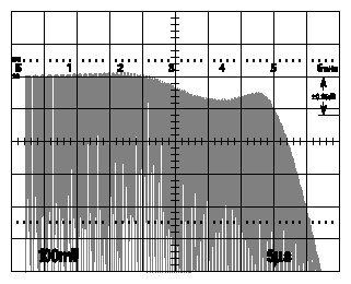
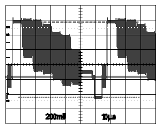
The input signal is an analog 700mVp-p frequency sweep, from 0.5 MHz to 5.75 MHz. The input operating mode is analog RGB, with 625 timing.
The passband ripple measures 0.50 dB p-p to 5.4 MHz. See Figure A-1 for a typical response. The sweep signal in the figure is measured at the input to the A/D converter and is more than 2.0 V p-p in amplitude.
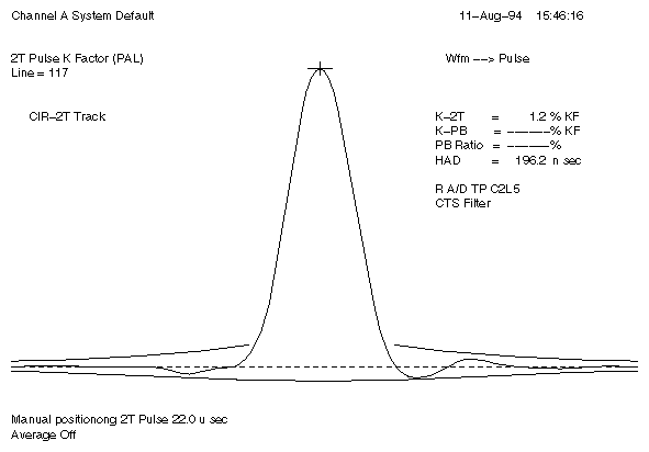
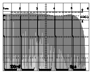
The input signal is an analog 700mVp-p (PAL) 2T Pulse with a HAD of 200 nsec. The input operating mode is analog RGB, with 625 timing.
The K-factor measurements ranged from 1.1-1.3% and averaged1.2% for a typical response; see Figure A-2. For an HAD of 250 nsec(NTSC), all channels would be <1.0%.
The K-factor measurements meet a <1% figure for NTSC 2T pulses.
The S/N ratio is measured at the input to the A/D converters. This includes the effects of the breakout box on the signals. Noise components can result from analog or digital crosstalk in the breakout box and on the Sirius VME board, and from thermal, excess, or popcorn noise sources within the circuitry.
First, measurements were taken with crosstalk effects eliminated as much as possible. A 50% gray flat field was applied to one channel at a time with no signals applied to the D1 inputs or to the inputs of the channels not being tested. Finally, 5.75 MHz full amplitude sweeps were applied to all analog input except for the input under test; simultaneously, D1 4:2:2:4 5.75 MHz full amplitude digital sweeps were applied to the D1 inputs. This second case is a worst-case scenario that does not represent normal operating conditions.
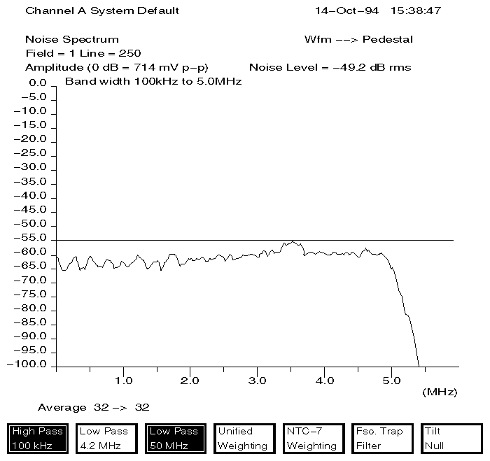
The S/N results summarized in Table A-2 were obtained with the VM700A and active probe modified for variable gain. A bandwidth of 100kHz-5.0 MHz was used with no weighting. The A/D input test points were the point of measurement. The specification is >=65 dB, weighted.
Table A-2. S/N Ratio, A/D Inputs, No Crosstalk, 100kHz-5.0 MHz, No Weighting
Channel | Green | Blue | Red | Alpha |
|---|---|---|---|---|
S/N | 66.8 dB | 66.6 dB | 66.4 dB | 66.5 dB |
Typical S/N ratio with crosstalk included is 55 dB.
A horizontal rate signal from the input genlock phase-locked loop was measured for jitter using a Hewlett-Packard time domain analyzer. This instrument measures peak-to-peak jitter and standard deviation jitter; it was set to collect data on 1000 samples.
The maximum peak-to-peak jitter was 9.8 nsec, with a standard deviation of 0.65 nsec. It was estimated that 95% of the samples had a peak-to-peak jitter of less than 4.0 nsec. These are good numbers for an H-rate genlock system.
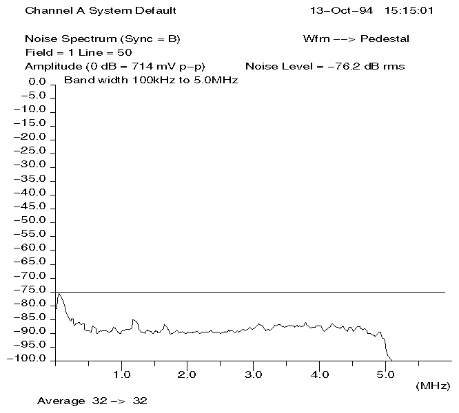
The input genlock circuit contains a mux that selects from the various possible genlock sources. Both the S/N ratio and crosstalk were measured by applying multiburst signals to the composite, R, G, B, alpha, and sync inputs. The house (genlock) input was selected as the output genlock source, but no signal was applied to this input. The input to the genlock A/D converter was then measured for S/N ratio, which includes crosstalk.
The resulting S/N ratio was 76 dB over a bandwidth of 100 kHz to 5.0 MHz, no weighting, and with averaging on. This indicates that there is a very high S/N ratio with negligible crosstalk.
Figure A-8 shows input genlock S/N ratio; crosstalk is worst-case and not comparable to normal operation. Multiburst was applied to the applied to R, G, B, A, composite, and sync inputs. On the mux, “house” was selected, with nothing connected to that input.
The quality of the composite and Y/C inputs was measured by inputting composite analog test signals and measuring the composite output signal. This technique measures the combined performance of signal decoding and encoding. The output signal quality was measured separately and is summarized later. The frequency response and S/N ratio using the Y/C inputs would be even better, due to the absence of chroma/luma separation. The encoder and decoder only process 8-bit video.
An NTSC multiburst signal was applied to the composite input (and to all other inputs) and measured on the composite output; Figure A-4. The frequency response is quite flat to beyond 2.0 MHz. Crosscolor, which is a normal effect, is visible on the last three bursts. The level of the signal, as well as the shape and amplitude of sync and burst, are correct.
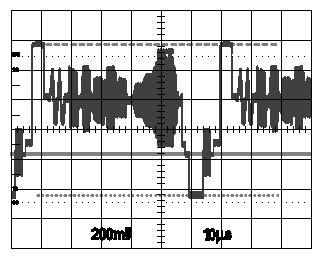
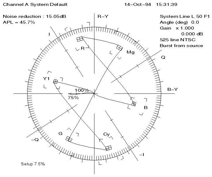
Figure A-5 shows the decoded and encoded 75% color-bar signal (TSG-100). Figure A-6 shows the vector display of this color-bar signal. Except for the slightly hot subcarrier level, the vector accuracy is within all of the small boxes, with negligible offset.
The S/N ratio of the composite in-out path was measured using a 50% gray field from a TSG-100 generator, and making the measurement with a VM-700A. Figure A-7 shows the results. A S/N ratio of -49 dB was obtained with a bandwidth of 10 0 kHz-5.0 MHz and no weighting.
This section discusses
frequency response
transient (K-factor) response
signal-to-noise ratio
output sync waveforms
output jitter
output genlock crosstalk
composite output
output timing
D1 4:2:2:4 video in, with measurements made on the G, B, R, and alpha output channels of the breakout box. The input operating mode is parallel 4:2:2:4 input with CCIR601 525 timing. The output operating mode is RGB output, also with CCIR601 525 timing. The D1 test signal is a full amplitude 5.75 MHz sweep signal. The RGB output sweep was measured on an oscilloscope with signal-to-noise ratio amplitude markers set for a 0.5 dB p-p spread.
The measured response under +-0.5 dB ripple conditions extends to 5.2 MHz with sinX/X correction, relative to 100kHz; see Figure A-8.
The measured response under 1.0 dB p-p ripple conditions extends to 5.5 MHz, relative to 100 kHz. The specification is +-0.5 dB to 5.5 MHz. This response includes SinX/X correction for the 601 sample clocks. For the square pixel 525 mode, the response will be down by an additional 0.1 dB at 5.0 MHz; for the square pixel 625 mode, the response will rise by an additional 0.08 dB at 5.0 MHz.
The output frequency response typically meets the specifications.
The input signal is a D1 4:2:2:4 PAL 2T Pulse with a HAD of 200 nsec. The output operating mode is analog RGB, with 625 timing.
The PAL K-factor measurements uniformly measured 0.8% for a typical response; see Figure A-9. For an HAD of 250 nsec (NTSC), all channels would be <0.8%.
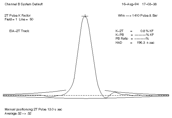
The output K-factor measurements meet a <1% figure for both NTSC and PAL 2T Pulses.
Disregarding crosstalk, the inherent S/N ratio of any of the R, G, B, or alpha channels is 78dB, measured 100kHz to 5.0MHz, with no weighting. The effect of output crosstalk on S/N ratio was measured by outputting a 5.75MHz sweep signal on the RGB and Alpha outputs, but disabling the output lookup table on one channel at a time, and measuring the S/N ratio of that channel. A bandwidth of 100 kHz to 5.0 MHz and no weighting was used. The results are summarized in Table A-3.
GB Alpha into R | GR Alpha into B | BR Alpha into G | GBR into Alpha |
|---|---|---|---|
65.2 dB | 63.8 dB | 68.4 dB | 56.7 dB |
| Note: These crosstalk conditions are worst-case and not comparable to normal operation, particularly because most alpha channel signals will not have the high-frequency content of the sweep signal. |
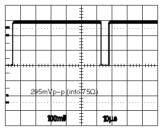
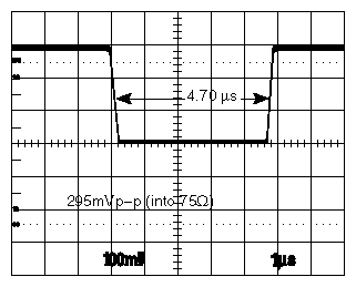
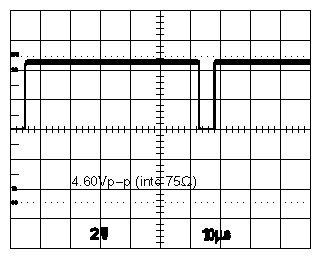
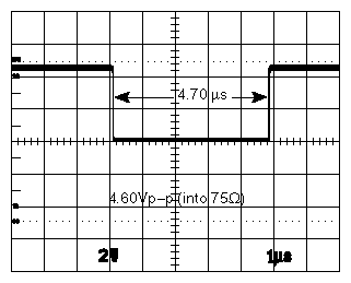
The output sync signal is available in either 300mVolt or TTL (4V) level, as controlled by software.
The 300mV version has a 75 Ohm output impedance and is measured into a 75 Ohm load. The level is very precise, with an accuracy of <3%, is Gaussian-shaped, and has a rise-fall time of 140 nsec (+-10%). Figure A-10, Figure A-11, and Figure A-12 show typical waveforms.
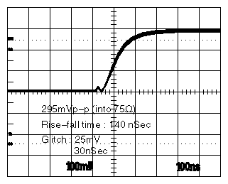
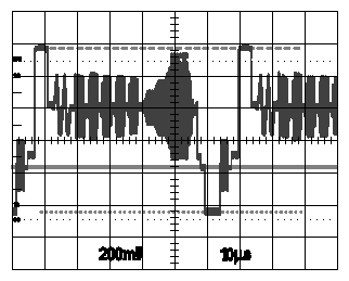
There is a small 25 mV 30 nsec glitch at the beginning of each transition; but this is unlikely to cause a problem with any external sync detector. The glitch is due to crosstalk around the TTL buffer that produces the 4V sync.
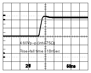
The 4 Volt sync output was designed to be terminated in a 75-Ohm load; with a typical amplitude of 4.5 V p-p +-.25V under these conditions. It has a rise-fall time of 18 nsec, and a very low output impedance. The DC level of sync tip is ground, the polarity is negative-going.
| Caution: When operating in the 4V mode, it is important to terminate the sync output with a 75-Ohm load, or excessive ringing will appear due to the EMI filter on the output of the breakout box. Figure A-13, Figure A-14, and Figure A-15 show typical waveforms. |
The output jitter was measured with a Tektronix VM700A video measurement set by measuring the video and sync waveforms on the output of the breakout box, and by a time domain analyzer (TDA) that measures jitter on TTL logic waveforms. The VM700A has a minimum jitter of 3 to 4 nsec, when measuring a high-quality generator output signal. Jitter was measured with no additional filtering on the VM700A, and with a 1.5 MHz Gaussian filter inserted in the path.
The output genlock jitter is very low, at approximately 1nsec measured with the TDA. The results shown in Table A-4 were obtained with the VM700A, and are for the CCIR 601 525/625 modes, with essentially the same results obtained for the square pixel 525/625 modes.
| Sync Out | G/Y Out | Composite Out |
|---|---|---|---|
NTSC: No filtering | 4 nsec | 12 nsec | 5 nsec |
NTSC: Gaussian filter | - | 5 nsec | 4 nsec |
PAL: No filtering | 7 nsec | 13 nsec | 15 nsec |
PAL: Gaussian filter | 4-5 nsec | 5 nsec | 10 nsec |
The SYNC OUT and GBRA/YUVA COMPONENT SYNC outputs on the breakout box have very low jitter when high frequency noise is filtered out. The jitter approaches the residual of 3-4 nsec. When correlated with the results of the TDA, the conclusion is that the non-filtered jitter is the result of high-frequency noise contaminating the video appearing at the breakout box outputs.
These conclusions also apply to NTSC composite output, which exhibits similar measurements as the Sync and component outputs. However, the PAL composite output has much higher jitter. This increased jitter is due to noise on the chroma output that occurs during the sync edge. The Y/C Luminance output signal does not have the noise, and does not exhibit the increased jitter. The noise on the chroma channel may be produced within the encoder chip.
By using the “square root of the sum of squares” formula, with a residual jitter measurement of 3.5 nsec and a measured jitter of 5 nsec, the output genlock jitter is calculated at 3.5 nsec. This is an acceptable figure for a line-locked system
Output genlock crosstalk and S/N ratio were measured by applying full amplitude 5.75 MHz sweep signals to all inputs except for either sync or house (genlock) input. The S/N ratio was measured at the analog input to the genlock circuit, with a bandwidth of 100 kHz to 5.0 MHz, no weighting, and averaging on. The S/N ratio was measured both on line 17, where there could be no crosstalk because it is not an active line, and on line 50, where there would be crosstalk. The output genlock mux was used to select either the sync or house input. Table A-5 summarizes these results.
Table A-5. Output Genlock Crosstalk
Genlock (House) Input |
| Sync Input |
|
|---|---|---|---|
Line 17 | Line 50 | Line 17 | Line 50 |
67.3dB | 64.7dB | 67.0dB | 59.3dB |
These results are worst-case conditions not comparable to normal operation. The 59 dB figure, when the sync input is selected, is due primarily to equal crosstalk from the green and composite inputs. This figure indicates that the house input is the preferable one to use to minimize crosstalk.
The quality of the composite and Y/C outputs was measured by inputting digital 601 75% color bars and outputting composite color bars.
Frequency response was measured by inputting a digital 601 5.75 MHz sweep signal and viewing the composite output. The response is flat to beyond 5.0 MHz, as seen in Figure A-16.
Digital 75% color bars were input to the system. In the composite output, the levels and appearance of the bars is correct, and the levels, shape, and timing of sync and burst are correct.
Figure A-19 shows the vector display of color bars, and shows a slightly hot subcarrier amplitude with excellent vector accuracy and negligible offset. A flat 50% gray field was applied to the digital 601 input and output on composite. Figure A-20 shows that the S/N ratio is 50 dB.
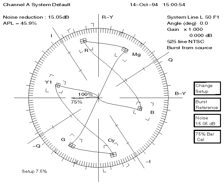
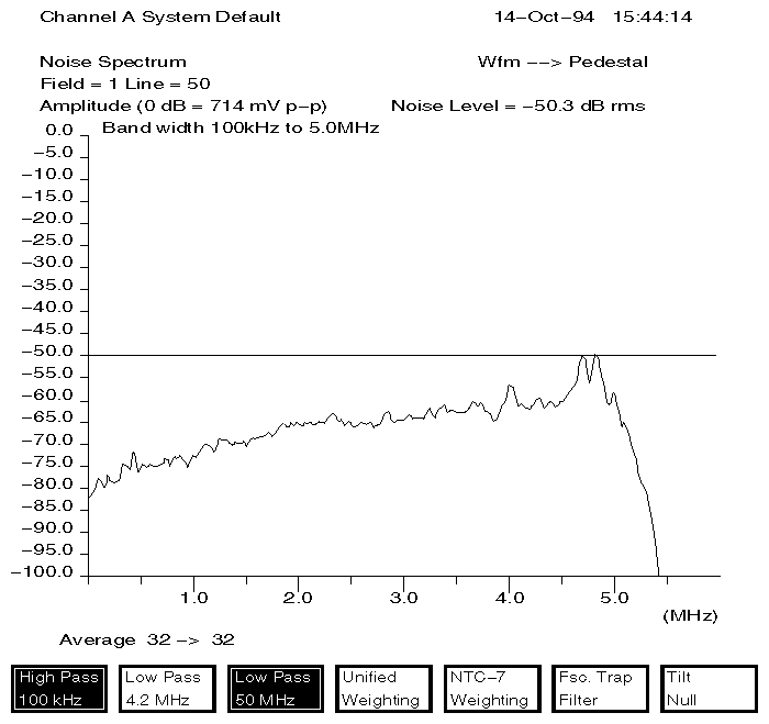
Figure A-19 and Figure A-20 show the output timing of green versus red, and green versus blue; and indicate that the channels are coincident. The input to the breakout box was composite color bars from a TSG-100 generator, and the output was RGB from the breakout box.
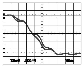

Table A-6 summarizes Sirius Video video formats.
Table A-6. Sirius Video Formats
Format | Video Stream | Tape Format |
|---|---|---|
Digital component | 4:4:4:4, 4:2:2:4, 4:2:2 | CCIR 601 (8/10 bits) |
Analog component | RGBA, YUVA, PrYPbA | Betacam, M-II, SMPTE;
10-bit ADC/DAC; |
Analog composite | 525 and 625 timings | NTSC, PAL, S-Video |
For more information, see the following standards, which contain provisions for video signals:
CCIR 601-2: Encoding Parameters of Digital Television for Studios (4:2:2 component video signals, single link)
ANSI/SMPTE 125M-1992: Television—Component Video Signal 4:2:2—Bit-Parallel Digital Interface
SMPTE Recommended Practice (RP) 175-1993: Digital Interface for 4:4:4:4 Component Video Signals (Dual Link)
SMPTE 259M, Television—10-Bit 4:2:2 Component and 4fsc NTSC composite Digital Signals—Serial Digital Interface
SMPTE RP 157-1990: Key Signals
Table A-7 summarizes the specifications for the host connections on the breakout box.
Table A-7. Breakout Box Host Connections
Connector Label | Definition/Specification |
|---|---|
ANALOG 2 | Analog cables to Sirius Video board via I/O door on workstation |
DIGITAL 1 | Digital cables to Sirius Video board via I/O door on workstation |
Power | Autoranging to accept voltage range shown |
Figure A-21 shows the Sirius Video breakout box.
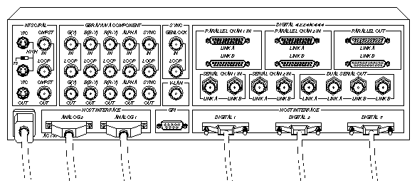
Table A-8 summarizes the breakout box connectors and switches that interface with video equipment.
Table A-8. Interface for Video Equipment
Section | Connector or Switch | Description |
|---|---|---|
NTSC/PAL | Y/C (loop)75/HIGHCMPST INLOOP | S-Video source (tape deck or camera) Self-termination switch for S-Video input Composite video input from tape deck or camera Loopthrough for each composite video input, with buffered signal to workstation S-Video output to tape deck or monitor Composite video destination (tape deck or monitor) |
GBRA/YUVA COMPONENT | G(Y) IN | Analog component (GBR or YUV plus alpha and
sync) video source (tape deck or camera) Loopthrough for each component video input, with buffered signals to workstation Analog component (GBR or YUV plus alpha and sync) video destination (tape deck or monitor) |
SYNC | GENLOCK INLOOP | External sync source (house sync) Loopthrough for genlock input with buffered signal to workstation |
V-LAN |
| V-LAN transmitter |
GPI |
| Graphics Peripheral Interface source/destination (tape deck or digital recorder); see Chapter 4, “Controlling the General-Purpose Interface (GPI),” for details. |
DIGITAL 4:2:2:4/4:4:4:4 | PARALLEL CHAN [1,2] INPARALLEL OUTSERIAL CHAN [1,2] INDUAL SERIAL OUT | Parallel digital video source (digital tape deck or other recording device) Parallel digital video destination (digital tape deck or other recording device) Serial digital video source, if optional serializer board (SD1) is installed in breakout box Serial digital video destination, if optional serial board (SD1) is installed in breakout box Note: The transfer mode (packing format) selected determines Link A and Link B usage, as explained in Table A-9. |
Table A-9 explains the use of Link A and Link B connectors in the DIGITAL 4:2:2:4/4:4:4:4 section of the breakout box. Each carries 10-bit wide YUVA.
Table A-9. Transfer Mode Usage for Link A and Link B Digital Connectors
4:2:2:4 Link A | 4:2:2:4 Link B | 4:4:4:4 Link A | 4:4:4:4 Link B |
|---|---|---|---|
Cb0 | x | Cb0 | Cb1 |
Y0 | A0 | Y1 | A0 |
Cr0 | x | Cr0 | Cr1 |
Y1 | A1 | Y1 | A1 |
If Link B is not used in 4:2:2:4 format, the resulting format is 4:2:2
Table A-10 summarizes Sirius Video video connectors.
Input | Output |
|---|---|
2 pairs of serial/parallel digital | 2 serial/parallel digital |
1 analog component | 1 analog component |
1 analog composite | 1 analog composite |
Sirius Video controls are
two GPI input lines
two GPI output lines
V-LAN interface
genlock/sync input
loopthroughs for all analog inputs