This appendix provides information to help users integrate third-party VME boards into the Onyx, Onyx R10000, and POWER Onyx rackmount systems. Hereinafter, the term Onyx is used to refer to all Onyx systems unless it is necessary to refer to a specific system type. The following information is divided into three major sections:
“VMEbus Architecture Interface,” provides a detailed discussion of the VMEbus architecture in the Onyx system. This section also briefly describes the overall bus structure, VME interrupt generation, and address mapping.
“Hardware Considerations,”discusses pertinent physical and electrical requirements and issues such as the required board dimensions, available power, airflow, VME pins assignments, the VME slots, and VME backplane jumpering.
“VMEbus Boards Design Considerations,” provides third-party VME board design considerations and guidelines.
| Note: This appendix primarily provides VMEbus hardware-related information. For software-related information on VMEbus implementation, consult the IRIX Device Driver Programming Guide (P/N 007-0911-xxx). |
The VME (versa modular European) interface in the Onyx and POWER Onyx rack systems supports all protocols defined in Revision C of the VME specification, plus the A64 and D64 modes defined in Revision D. For the acceptable VME address ranges, read the /var/sysgen/system/irix.sm file.
| Note: The Onyx system does not support VSBbus mode. |
| Warning: All board installations or removals should be performed only by personnel trained, certified, or approved by Silicon Graphics. Unauthorized access to the card cage area could result in system damage, or possible bodily harm, and could void the warranty for the system. |
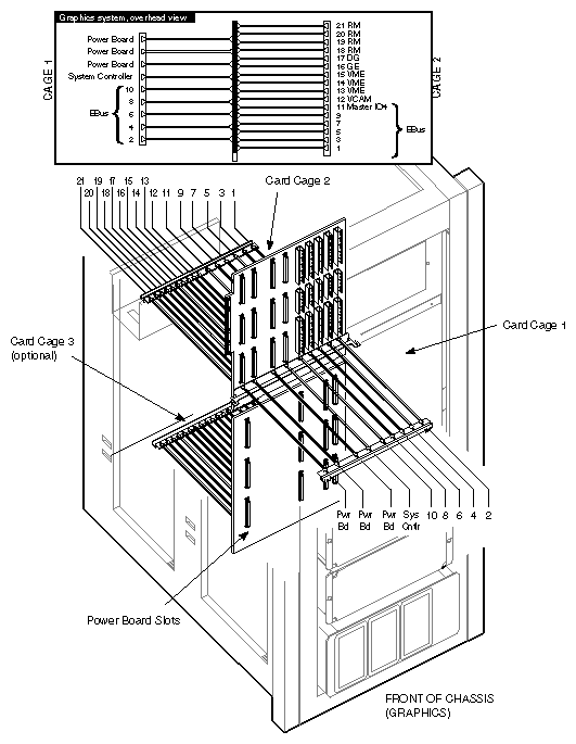
The VMEbus interface circuitry for the Onyx and POWER Onyx systems resides on a mezzanine board called the VMEbus Channel Adapter Module (VCAM) board. The VCAM board is standard in every system and mounts directly on top of the IO4 board in the system card cage (see Figure E-1). The VCAM is located on the master IO4 (in slot 12) and provides the VME connection for card cage 2.
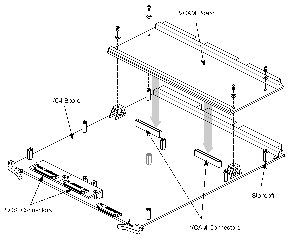
The IO4 board is the heart of the I/O subsystem. The IO4 board supplies the system with a basic set of I/O controllers and system boot and configuration devices such as serial and parallel ports and Ethernet.
In addition, the IO4 board provides these interfaces:
two flat-cable interconnects (FCIs) for connection to the CC3
two SCSI-2 cable connections
two Ibus connections
See Figure E-2 for a functional block diagram of the IO4 board.
This section describes the bus structure of the system.
The main set of buses in the Onyx system architecture is the Everest address and data buses, Ebus for short. The Ebus provides a 256-bit data bus and a 40-bit address bus that can sustain a bandwidth of 1.2 GB per second.
The 256-bit data bus provides the data transfer capability to support a large number of high-performance RISC CPUs. The 40-bit address bus is also wide enough to support 16 GB of contiguous memory in addition to an 8 GB I/O address space.
The 64-bit Ibus (also known as the HIO bus) is the main internal bus of the I/O subsystem and interfaces to the high-power Ebus through a group of bus adapters.The Ibus has a bandwidth of 320 MB per second that can sufficiently support a graphics subsystem, a VME64 bus, and as many as eight SCSI channels operating simultaneously.
Communication with the VME and SCSI buses, the installed set or sets of graphics boards, and Ethernet takes place through the 64-bit Ibus (see Figure E-2). The Ibus interfaces to the main system bus, the 256-bit Ebus, through a set of interface control devices, an I address (IA) and four I data (ID). The ID ASICs latch the data, and the IA ASIC clocks the data from each ID to the Flat Cable Interface (FCI) through the F controller (or F chip).
Two FCI controllers (or F controllers) help handle the data transfers to and from an internal graphics board set (if applicable) and any VMEbus boards in optional CC3 applications. The SCSI-2 (S1) controller serves as an interface to the various SCSI-2 buses. The Everest peripheral controller (EPC) device manages the data movement to and from the Ethernet, a parallel port, and various types of on-board PROMs and RAM.
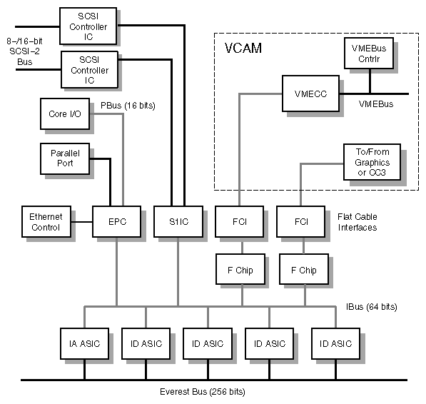
The VCAM board provides the interface between the Ebus and the VMEbus and manages the signal level conversion between the two buses. The VCAM also provides a pass-through connection that ties the graphics subsystem to the Ebus.
The VCAM can operate as either a master or a slave. It supports DMA-to-memory transactions on the Ebus and programmed I/O (PIO) operations from the system bus to addresses on the VMEbus. In addition, the VCAM provides virtual address translation capability and a DMA engine that increases the performance of non-DMA VME boards.
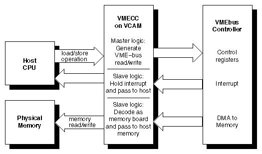
The VMECC (VME cache controller) gate array is the major active device on the VCAM. The VMECC interfaces and translates host CPU operations to VMEbus operations (see Figure E-3). The VMECC also decodes VMEbus operations to translate them to the host side.
The VMECC provides the following features:
an internal DMA engine to speed copies between physical memory and VME space
a 16-entry deep PIO FIFO to smooth writing to the VME bus from the host CPUs
a built-in VME interrupt handler and built-in VME bus arbiter
an explicit internal delay register to aid in spacing PIOs for VME controller boards that cannot accept back-to-back operations
A16, A24, A32, and A64 addressing modes (see Table E-1) that can be issued as a bus master with PIOs
single-item transfers (D8, D16, D32, and D64) that can be issued as a bus master with PIOs
A24, A32, and A64 addressing modes that can be responded to as a memory slave to provide access to the Ebus
single-item transfers (D8, D16, and D32) that can be responded to as a memory slave to provide access to the Ebus
block-item transfers (D8, D16, D32, and D64—see Table E-1) that can be responded to as a memory slave
Table E-1. Supported Address and Data Sizes
Size
Term
A16 and D8 modes
Short
A24 and D16 modes
Standard
A32 and D32 modes
Extended
A64 and D64 modes
Long
The VMECC also provides four levels of VMEbus request grants, 0-3, (3 has the highest priority), for DMA arbitration. Do not confuse these bus request levels with the interrupt priorities described in “VMEbus Interrupts.” Bus requests prioritize the use of the physical lines representing the bus and are normally set by means of jumpers on the interface board.
Data transfers between VME controller boards and the host CPU(s) takes place through the VMECC on the VCAM board, then through a flat cable interface (FCI), and onto the F controller ASIC.
The F controller acts as an interface between the Ibus and the Flat Cable Interfaces (FCIs). This device is primarily composed of FIFO registers and synchronizers that provide protocol conversion and buffer transactions in both directions and translate 34-bit I/O addresses into 40-bit system addresses.
Two configurations of the F controller are used on the IO4 board; the difference between them is the instruction set they contain. One version is programmed with a set of instructions designed to communicate with the GFXCC (for graphics), the other version has instructions designed for the VMECC. All communication with the GFXCC or VMECC ICs is done over the FCI, where the F controller is always the slave.
Both versions of the F controller ASICs have I/O error-detection and handling capabilities. Data errors that occur on either the Ibus or the FCI are recorded by the F controller and sent to the VMECC or GFXCC.
ICs must report the error to the appropriate CPU and log any specific information about the operation in progress). FCI errors are recorded in the error status register. This register provides the status of the first error that occurred, as well as the cause of the most recent FCI reset.
The Onyx and POWER Onyx VMEbus interface supports all protocols defined in Revision C of the VME specification plus the A64 and D64 modes defined in Revision D. The D64 mode allows DMA bandwidths of up to 60 MB. This bus also supports the following features:
seven levels of prioritized processor interrupts
16-bit, 24-bit, and 32-bit data addresses and 64-bit memory addresses
16-bit and 32-bit accesses (and 64-bit accesses in MIPS III mode)
8-bit, 16-bit, 32-bit, and 64-bit data transfer
DMA to and from main memory
The VME bus does not distinguish between I/O and memory space, and it supports multiple address spaces. This feature allows you to put 16-bit devices in the 16-bit space, 24-bit devices in the 24-bit space, 32-bit devices in the 32-bit space, and 64-bit devices in 64-bit space.[1]
The VME bus provides 32 address bits and six address-modifier bits. It supports four address sizes: 16-bit, 24-bit, 32-bit, and 64-bits (A16, A24, A32, and A64). The VME bus allows the master to broadcast addresses at any of these sizes. The VME bus supports data transfer sizes of 8, 16, 32, or 64 bits.
| Note: To best understand the VME-bus addressing and address space, think of the device as consisting of two halves, master and slave. When the CPU accesses the address space of a device, the device acts as a VME slave. When the VME device accesses main memory through direct memory access operations, the VME device acts as a VME master. |
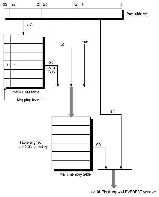
In the Onyx and POWER Onyx systems, a DMA address from a VME controller goes through a two-level translation to generate an acceptable physical address. This requires two levels of mapping. The first level of mapping is done through the map RAM on the IO4 board. The second level is done through the map tables in system memory. This mapping is shown in Figure E-4.
| Note: The second level mapping requires system memory to be reserved for the mapping tables. The current limit on the number of pages that is allocated for map tables is 16 pages and the maximum memory allotted for the map tables is 64 KB. The R4400 provides a 4 KB page size for 16 pages (4 KB * 16 pages= 64 KB). The R8000 provides an 8 KB page size for 8 pages (8 KB * 8 pages = 64 KB). |
The R4400 pointer size is 4 bytes and the R8000 pointer size is 8 bytes. There are 1K mapping entries for the R4400 for each page and 8K mapping entries in the R8000. In the R4400, if you divide the amount of memory allocated for the map tables (64 KB) by the pointer size (4 B) and then multiply it by the page size (4 KB), you derive 64 MB of VME DMA mapping. This is the maximum allowed by IRIX. The 64 MB address space applies to the R8000, as well.
Referring to the top of Figure E-4, bits 32 and 33 from the IBus address come from the VMECC. These two bits determine a unique VMEbus number for systems with multiple VMEbusses. Of the remaining 32 bits (31 to 0), 12 are reserved for an offset in physical memory, and the other 20 bits are used to select up to 220 or 1 million pages into the main memory table. However, as stated earlier only 64 KB is allocated for map tables.
As shown in Figure E-4, 13 bits go to the static RAM table. Recall that two of the thirteen bits are from the VMECC to identify the VMEbus number. The static RAM table then generates a 29-bit identifier into the main memory table. These 29 bits select a table in the main memory table. An additional nine bits select an entry or element within the table. A 00 (two zeros) are appended to form a 40-bit address into the main memory table.
The main memory table then generates 28-bit address which is then appended to the 12-bit offset of the IBus to form the final 40-bit physical address.
| Note: Address conflicts with other boards in the system should not be a problem as long as the drivers and the VME controllers adhere to the semantics for DMA mapping defined in the IRIX Device Driver Programming Guide (p/n 007-0911-xxx). |
This section describes the VMEbus operation for the following address and data cycles:
write (non-block)
read (non-block)
read-modify-write (issued only by the VMECC)
Table E-2 shows the word length conventions used in this document.
Table E-2. Word Length Conventions
Parameter | Number of Bits |
|---|---|
Byte | 8 bits |
Half-word | 16 bits |
Word | 32 bits |
Double or long word | 64 bits |
The write cycle begins when the master gets the bus and asserts WRITE*. The master places the address on the address bus (A01 to A31) and also places the address modifier on the bus (AM0 through AM5) to indicate the type of access and address space (for example A16, A24, A32, or A64). The address strobe (AS*) is then asserted to indicate a stable address.
The master then places the data on the data bus (D00 through D31) and asserts the data strobes DS0* AND DS1* and LWORD*. This combination determines the data size (for example, D32, D16, or D8).
The slave takes the data and responds by asserting the DTACK* line. When the master releases the data strobes, (DS0* and DS1*), the slave releases DTACK* and the cycle is completed, as the AS* signal is released. If a mismatch in the data transfer size or other errors occur, the slave asserts BERR* and the bus error terminates the cycle.
The read cycle is the same as the write cycle except that the slave places the data on the data bus (D00 through D31) in response to data strobes and long word combinations (DS0, DS1, and LWORD) from the host CPU. The slave asserts DTACK* when the data is driven and the master reads it. The master then releases the strobe and the slave releases DTACK* and AS, and the cycle is completed.
The read-modify-write (or RMW) allows a master to read data, modify it, and write it back without releasing the bus. This bus cycle allows users to read and change the contents of a device register or memory location in a single atomic operation. Although this feature is typically used to implement synchronization primitives on VME memory, you may occasionally find this feature useful for certain devices.
| Note: Silicon Graphics products do not support VME read-modify-write operations initiated by a VME master to host memory. |
The VME bus supports seven levels of prioritized interrupts, 1 through 7 (where 7 has the highest priority). The VMECC has a register associated with each level. When the system responds to the VMEbus interrupt, it services all devices identified in the interrupt vector register in order of their VMEbus priority (highest number first). The operating system then determines which interrupt routine to use, based on the interrupt level and the interrupt vector value.
| Note: On systems equipped with multiple VME buses, adapter 0 has the highest priority; other adapters are prioritized in ascending order (after 0). |
No device can interrupt the VME bus at the same level as an interrupt currently being serviced by the CPU because the register associated with that level is busy. A device that tries to post a VME-bus interrupt at the same VME-bus priority level as the interrupt being serviced must wait until the current interrupt is processed.
| Note: All VME interrupt levels map into one CPU interrupt level through IRIX. |
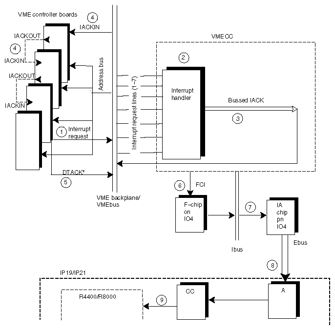
The following and Figure E-5 outline how a VMEbus interrupt is generated.
A VME controller board asserts a VME interrupt.
The built-in interrupt handler in the VMECC chip checks if the interrupt level is presently enabled by an internal interrupt mask.
The interrupt handler in the VMECC issues a bussed IACK (interrupt acknowledge) response and acquires the vector from the device. The 3-bit response identifies one of the seven VME address.

Note: Once an interrupt is asserted and the bus is granted to the handler, a 3-bit code that identifies the interrupt level being acknowledged is placed on address bits 1 to 3 and IACK* and AS* are asserted.
If multiple VME boards are present, the bused IACK signal is sent to the first VME controller as an IACKIN. As shown in Figure E-5, since the first controller is not the requesting master, it passes the IACKIN signal to the next board (in the daisy-chain) as IACKOUT.
Note: Each board compares the interrupt level with the interrupt level it may or may not have asserted. If the board did not generate an interrupt, or if the interrupt level does not match its own level, the board passes on the IACKOUT signal to the next board. In addition, the board closest to the master IO4 normally wins access to the bus.
The requesting board responds by issuing an DTACK* (data acknowledge signal), blocking the IACKOUT signal to the next board in line (if present), and placing an 8-bit status word on the data bus.
After acceptance and completion through the VMECC, the interrupt signal is sent over the FCI interface to the F-chip and is queued awaiting completion of other F-chip tasks.
The F-chip (or F controller ASIC) requests the I-bus and sends the interrupt to the IA chip.
The IA chip requests the Ebus and sends the interrupt over the Ebus to the CC chip on the CPU board.
The CC chip interrupts the CPU, provided that the interrupt level is not masked.
While the interrupt handler is executing, it prevents another interrupt at an equal or lower level from being serviced. Furthermore, all pending interrupts that are equal to or higher than the priority of a new interrupt must complete execution before the new interrupt is serviced.
The time for this to complete is normally less than 3 microseconds, but will be queued to await completion of other VME activities.
VME boards have two methods of interrupt acknowledge:
release on acknowledge of interrupt
release on register acknowledge of interrupt
The first release policy is where the interrupting device removes the IRQ request once the VMECC acknowledges the interrupt. In other words, the VME board assertion of the IRQ line is dropped when the board transfers its interrupt vector to the VMECC.
The second release policy occurs when the interrupting VME board does not drop the IRQ line the until a register on the board has been accessed or modified. Therefore, after the interrupt vector has been transferred, the device still asserts IRQ.
The following outlines VME interrupt problems that could result in VME interrupt error messages, such as: WARNING: stray VME interrupt, vector=0xff.
Noise occurs on one of the IRQ lines. If the noise pulse (signal) is wider than 20 ns, then the VMECC attempts to issue an IACK cycle. If the signal is just noise and not an actual interrupt, no expectant response to the IACK takes place. This lack of a response from a VME board results in a time out, causing the VMECC to issue an eventual error message.
A VME board accidentally asserts an IRQ line and doesn't respond.
One of the boards in front of the requesting board improperly blocks the IACKIN signal and doesn't respond.
The VMECC responds only to those interrupt levels that it is configured to recognize. You can therefore prevent the VMECC from responding to particular interrupt levels. For example, if the kernel is configured to have two VME devices configured at ipl=3 and 4, then the VMECC responds to interrupt levels 3 and 4 only. The VMECC does not respond to any other interrupt levels thereafter.
The VMEbus supports two arbitration schemes: priority and round robin. The VMECC designates the highest priority to its internal bus masters, the interrupt handler, and the PIO master. These two bus masters have a higher priority than the four backplane request levels (BRQ3 through BRQ0). BRQ3 has the highest priority level. BRQ2 through BRQ0 use round-robin arbitration.
The master relinquishes the bus based on an internal policy of release on request or release when done. Most VME masters can set their arbitration scheme through jumper selectors or by software.
In round-robin scheduling, the arbitration keeps track of the history of the bus grants to different levels. The last bus request level to have the bus becomes the lowest priority. For example, if the bus current request level is 1, all bus request level 1s are pushed back to the end of the queue, after a bus grant. The bus request level that is adjacent to the lowest priority then becomes the highest priority.
As an example, at a given time, say that level 3 is currently the highest priority. After a bus grant takes place, level 3 then becomes the lowest priority, and level 2 (since it was previously adjacent to level 3) is now the highest bus-level priority.
This section defines physical and electrical parameters for implementing VMEbus boards and also provides VMEbus slot-specific information for the Onyx and POWER Onyx systems.
The Onyx board slots have a 9U (vertical) form factor and measure 15.75 inches (400 mm) horizontally. The board edges must also be less than or equal to 0.062 inches (1.57 mm). If the board is thicker, the edge of the board must be milled to fit into the card guide. In addition, the center-to-center board spacing is 0.8 inch (20.3 mm).
| Note: If you wish to install a 6U form-factor VMEbus board into the system, you need to obtain a 6U to 9U converter board from Silicon Graphics. See “Using a 6U to 9U Converter Board”, for further information. |
Card cage 2 has three available VME slots and supplies approximately 40 watts of +5-V power per VME slot (nominally) and also receives approximately 200 to 250 linear feet per minute (LFM) of air flow.
When using an InfiniteReality rackmount system with large numbers of processor, memory, graphics, and I/O boards; system power availability may limit the number of VME boards you can install. Table E-3 gives examples of the number of VME boards usable in CC1 and CC2 maximum configuration InfiniteReality systems.
| Note: There are no VME slots in the card cage 1 in the Onyx or POWER Onyx systems. |
Table E-3. CC1 and CC2 InfiniteReality Maximum Configuration Examples
CPU Bds. | Memory Bds. | IO4 Bds. | RM Bds. | VO2 Bds.[a] | VME Bds. |
|---|---|---|---|---|---|
6 | 2 | 1 | 4 | 2 | 1 |
6 | 4 | 1 | 2 | 2 | 1 |
6 | 4 | 1 | 4 | 1 | 0 |
5 | 3 | 2 | 4 | 2 | 1 |
5 | 2 | 3 | 4 | 2 | 1 |
5 | 4 | 1 | 4 | 2 | 1 |
4 | 2 | 4 | 4 | 2 | 1 |
[a] The Sirius (VO2) board installs in a VME slot and uses VME power. | |||||
| Note: Reducing the configuration by removing one memory board and one IO4 board allocates power for one additional CPU board. Removing one VO2 board from the configuration allows installation of two additional VME boards. |
The InfiniteReality card cage 3 (CC3), uses different power boards and has different limitations than the RE2 CC3 version. Use the information in Table E-4 when installing a fully configured card cage 3 (2 pipes with 4 RMs each).
Note that with only 250 total watts of (+5 V) VME power available, you can install a very limited (or 0) number of VME boards in a fully loaded CC3.
Table E-4. InfiniteReality CC3 VME Power Availability
CC3 Power Boards | +5V VME Power Available | +12V VME Power Available |
|---|---|---|
Five 303s and one 512T | 50 amps (250 watts) | 15 amps (180 watts) |
Because the high-performance graphics of the InfinteReality system consume more power than RealityEngine2 graphics; some maximum configurations preclude the installation of any VME boards.
| Note: The following four tables provide examples of maximum configurations of VME and all other types of boards supported in the rack system. In the case of a maximum system configuration, installation of additional boards in any card cage must be balanced by removal of a board or boards requiring equal power. For example: |
one memory board and one IO4 board = one CPU board
one VIO2 (Sirius) board = two VME boards
Table E-7 shows the limits of a fully configured InfiniteReality system using three graphics pipes with four RM6s in each pipe.
Table E-5. System Maximum (12 RM6s) Board Configuration
CPU Bds. | Memory Bds. | IO4 Bds. | RM Bds. | VO2 Bds. | VME Bds. |
|---|---|---|---|---|---|
5 | 2 | 3 | 12 | 0 | 0 |
4 | 2 | 3 | 12 | 1 | 0 |
3 | 2 | 3 | 12 | 2 | 1 |
2 | 1 | 3 | 12 | 4 | 1 |
Table E-7 shows the limits of an InfiniteReality system using three graphics pipes, with four RM6s in two pipes, and two RM6s in the third pipe.
Table E-6. System Maximum (10 RM6s) Board Configuration
CPU Bds. | Memory Bds. | IO4 Bds. | RM Bds. | VO2 Bds. | VME Bds. |
|---|---|---|---|---|---|
6 | 2 | 3 | 10 | 4 | 2 |
5 | 2 | 3 | 10 | 3 | 0 |
4 | 1 | 3 | 10 | 4 | 2 |
Table E-7 shows the limits of an InfiniteReality system using three graphics pipes, with four RM6s in one pipe, and two RM6s in the second and third pipes. Note that the configurations shown in Table E-7 may require a power board upgrade in CC3 to successfully support the large numbers of VO2 and VME boards listed in the example. Check with your Onyx service provider.
Table E-7. System Maximum (8 RM6s) Board Configuration
CPU Bds. | Memory Bds. | IO4 Bds. | RM Bds. | VO2 Bds. | VME Bds. |
|---|---|---|---|---|---|
6 | 2 | 3 | 8 | 4 | 2 |
5 | 2 | 3 | 8 | 5 | 2 |
4 | 2 | 3 | 8 | 6 | 2 |
Table E-7 shows the limits of an InfiniteReality system using two graphics pipes, with four RM6s in each pipe.
Table E-8. Two-Pipe System Maximum (8 RM6s) Board Configuration
CPU Bds. | Memory Bds. | IO4 Bds. | RM Bds. | VO2 Bds. | VME Bds. |
|---|---|---|---|---|---|
6 | 2 | 3 | 8 | 4 | 3 |
5 | 4 | 2 | 8 | 4 | 4 |
The card cage 3 (CC3), which is optional on the Onyx rackmount system, supplies up to 6 additional VME slots. The CC3 provides approximately
70 watts of +5-V power per VME slot. This assumes the presence of the proper power boards in the CC3 backplane. The power boards are included with the optional RE2 CC3 upgrade. The card cage 3 also receives approximately 200 to 250 linear feet per minute (LFM) of air flow through the chassis.
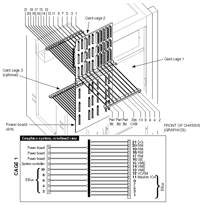
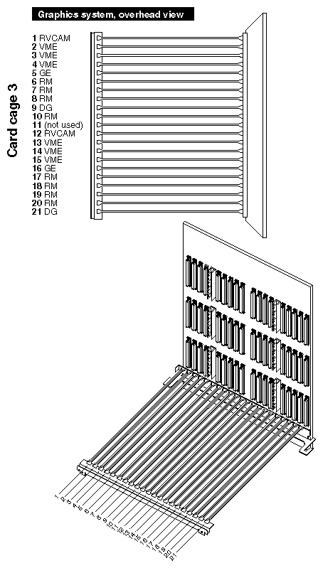
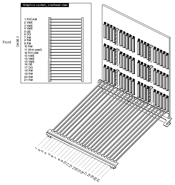
As mentioned earlier, card cage 1 has no available VME slots. Figure E-6 shows the card cage 1 and 2 slot assignments for the Onyx InfiniteReality rackmount system. Figure E-7 provides the optional CC3 slot assignments for InfiniteReality.
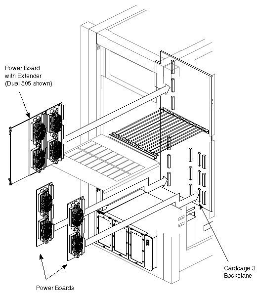
See Figure E-8 for an example of the power board locations in a rackmount Onyx system. Figure E-9 shows the location of the VME slots in card cage 2 in RealityEngine2 systems. See Figure E-10 for the optional card cage 3 slot assignments for RealityEngine2 systems.
If a VME board requires more than the normal slot power allotment (approximately 40 watts of +5 V power per slot in CC2 or approximately 70 watts in a card cage 3), the board still can be used providing that the following cooling and power guidelines are met.
The user needs to ensure that the board has the proper air flow (for cooling purposes) and sufficient available power. To help maintain proper cooling (according to manufacturer's specifications), the board may need special custom baffles or a set of non-component, enclosure boards to surround the VME board with sufficient air flow.
| Note: These custom air flow devices must be supplied by the customer. |
VME Power Guidelines
To use a third-party VME board that requires more than the normal VME slot power, be sure to observe these guidelines:
The board does not draw more than the amount of power allocated for VME board use.
The board does not exceed the power rating for the VME pins (approximately 200 watts).
The board uses all three "P" connectors on the system backplane: the P1, P2, and P3. See Table E-9 through Table E-11) for pinout information.
If these guidelines are followed along with the proper cooling requirements, a single VME board can draw as much as 150 watts of +5 V power.
In card cage 2, you can install two 75-watt VME boards (providing the boards are sufficiently cooled). However, as a result, you cannot install any additional VME boards, since the VME power allotment would already be saturated. It is also possible to use a single 150-watt VMEbus board in card cage 2, providing the remaining VME slots are also not used.
In the VME version of card cage 3, you can install up to nine 150-watt boards, assuming that all potential power boards (three 505 and one 512) are installed (see Figure E-8). However, as a result, the remaining VME slots cannot then be used.
Table E-9 through Table E-11 list the pin assignments of the VME P1, P2, and P3 connectors. Table E-12 describes the pin signals.
| Note: No connections are made to rows A and C of connector P2. These lines are not bussed across the backplane. The P3 connector uses the SunTM power convention. In addition, the Onyx system does not generate ACFAIL* or SYSFAIL*. The SERCLK and SERDAT* are also unused. |
The Onyx system supplies the defined voltages to the bus, also asserts SYSREST*, and drives SYSCLK (SYSCLK is driven at 16 MHz).
On the Onyx backplanes, the unused VME pins are no connects.
| Caution: The Onyx system does not support VSBbus boards. |
Table E-9. P1 VME Pin Assignments
Pin | Row A | Row B | Row C |
|---|---|---|---|
1 | D00 | BBSY* | D08 |
2 | D01 | BCLR* | D09 |
3 | D02 | ACFAIL | D10 |
4 | D03 | BG01N* | D11 |
5 | D04 | BG0OUT* | D12 |
6 | D05 | BG1IN* | D13 |
7 | D06 | BG1OUT* | D14 |
8 | D07 | BG2IN* | D15 |
9 | GND | BG2OUT* | GND |
10 | SYSCLK | BG3IN* | SYSFAIL* |
11 | GND | BG3OUT* | BERR* |
12 | DS1 | BR0* | SYSRESET* |
13 | DS0 | BR1 | LWORD* |
14 | WRITE* | BR2* | AM5 |
15 | GND | BR3* | A23 |
16 | DTACK* | AM0 | A22 |
17 | GND | AM1 | A21 |
18 | AS* | AM2 | A20 |
19 | GND | AM3 | A19 |
20 | IACK* | GND | A18 |
21 | IACKIN* | SERCLK | A17 |
22 | IACKOUT* | SERDAT* | A16 |
23 | AM4 | GND | A15 |
24 | A07 | IRQ7* | A14 |
25 | A06 | IRQ6* | A13 |
26 | A05 | IRQ5* | A12 |
27 | A04 | IRQ4* | A11 |
28 | A03 | IRQ3* | A10 |
29 | A02 | IRQ2* | A09 |
30 | A01 | IRQ1* | A08 |
31 | -12V | +5VSTDBY | +12V |
32 | +5V | +5V | +5V |
Table E-10. P2 VME Pin Assignments
Pin | Row A [a] | Row B | Row Ca |
|---|---|---|---|
1 |
| +5V |
|
2 |
| GND |
|
3 |
| RESERVED |
|
4 |
| A24 |
|
5 |
| A25 |
|
6 |
| A26 |
|
7 |
| A27 |
|
8 |
| A28 |
|
9 |
| A29 |
|
10 |
| A30 |
|
11 |
| A31 |
|
12 |
| GND |
|
13 |
| +5V |
|
14 |
| D16 |
|
15 |
| D17 |
|
16 |
| D18 |
|
17 |
| D19 |
|
18 |
| D20 |
|
19 |
| D21 |
|
20 |
| D22 |
|
21 |
| D23 |
|
22 |
| GND |
|
23 |
| D24 |
|
24 |
| D25 |
|
25 |
| D26 |
|
26 |
| D27 |
|
27 |
| D28 |
|
28 |
| D29 |
|
29 |
| D30 |
|
30 |
| D31 |
|
31 |
| GND |
|
32 |
| +5V |
|
[a] This row is user-defined. | |||
Table E-11. P3 VME Pin Assignments
Pin | Row A | Row B | Row C |
|---|---|---|---|
1 through 25 | +5V | Not connected | GND |
26, 27 | +12V | Not connected | +12V |
28, 29 | -12V | Not connected | -12V |
30 through 32 | -5V | Not connected | -5V |
| Note: In the Onyx VME backplanes, P3B is used for Silicon Graphics purposes. |
Table E-12. Signal Definitions
Signal Name | Definition |
|---|---|
D00 through D31 | Data lines. These lines are tri-stated and are not defined until the data strobes (DS0* and DS1*) are asserted by the MASTER. |
A00 through A31 | Address lines. These lines are tri-stated and are not defined until the address strobe (AS*) is asserted by the MASTER. |
AM0 through AM5 | Address modifier lines. Asserted by the MASTER and indicate the type of data transfer to take place. VME SLAVEs look at the lines to determine if they will respond and what type of response to make. |
DS0, DS1 | Data Strobe lines. Asserted by the MASTER and indicates stable data on the data bus. |
AS | Address strobe. Asserted by the MASTER and indicates a stable address is present on the address lines. |
BR0 through BR3 | Bus request lines. MASTER request a busy bus via these prioritized levels. |
BG0IN through BG3IN | Bus grant in (daisy-chained). |
BG0OUT through BG3OUT | Bus grant out (daisy-chained). |
BBSY | Bus busy. |
BCLR | Bus clear. (Hint to bus master: VME MASTERs are not required to comply) |
IRQ1 - IRQ7 | Interrupt request lines. |
IACK | Interrupt acknowledge. Asserted by MASTER to indicate the VME interrupt level to be serviced. |
IACKIN | Interrupt acknowledge in (daisy-chained). |
IACKOUT | Interrupt acknowledge out (daisy-chained.) |
DTACK | Data transfer acknowledge. Asserted by SLAVE to indicate a successful bus transfer. |
WRITE | Write not or read. |
LWORD | Indicates long word transfer (D32). |
SYSCLK | 16 MHz system clock. (Does not control bus timing.) |
SERCLK | Serial data clock. |
SERDAT | Serial data line. |
BERR | Bus error line. |
SYSFAIL | Indicates a board has failed. |
ACFAIL | AC power failure notify line. |
SYSRESET | Reset signal for VME bus. |
Skipping a slot is occasionally required to fit oversized VME boards or to improve air flow. A slot can be skipped if jumper blocks are placed on the appropriate VME jumper block pins.
| Note: If you install the VME boards in order (from left to right), then no jumpering is required. In addition, if you have no VME boards installed, you do not need to install any jumpers. |
The general guideline is to have jumpers into the jumper banks corresponding to the VME slot number that you are skipping (see Table E-13). For example, if you are skipping VME slot 13, you need to insert five jumpers into jumper bank 1 (see Figure E-11).
Table E-13. Correspondence of VME Jumpers to VME Slots
Jumper Bank | Cardcage 2 VME Slot |
|---|---|
1 | 13 |
2 | 14 |
3 | 15 |
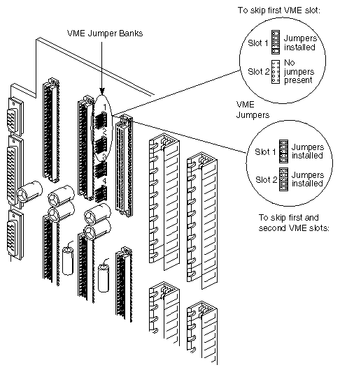
The optional card cage 3 VMEbus backplane does not have jumper banks as the midplane does. Skipped VMEbus slots in card cage 3 are jumpered using PCA CC3 VME jumper board (p/n 030-0516-001) from the card cage side.
| Caution: You must install this board only in the top VME connector, P1, or else damage may occur to the system. Bus jumpers are signals on the P1 connector. |
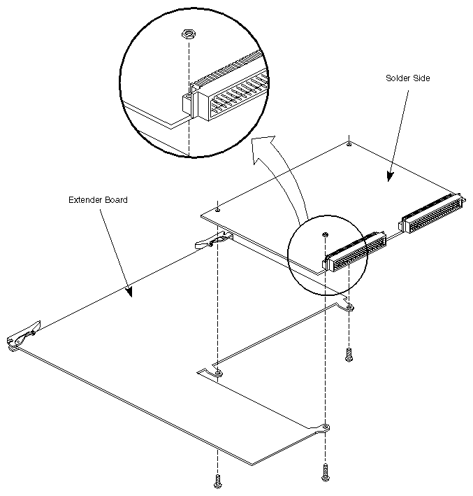
Some third-party VMEbus boards have a 6U form factor and require a Silicon Graphics 6U to 9U converter (or extender) board assembly to be used in the Onyx or POWER Onyx system (see Figure E-12).
| Note: Contact your Silicon Graphics sales office to obtain a 6U converter board (p/n 030-0519-001). |
This section provides design guidelines for implementing third-party VME boards. Be sure to observe these general rules to avoid possible damage to the VMEbus and system.
Devices should require 8-bit interrupt vectors only. This is the only interrupt vector size that is recognized by the IRIX kernel.
Devices must not require UAT (unaligned transfers or tri-byte) access from the Onyx system.
Devices in Slave mode must not require address modifiers, other than Supervisory/Nonprivileged data access.
While in VME Master mode, devices must access the system memory using Nonprivileged data access or Nonprivileged block transfers only.
Devices must have the ability to be configured so that their address range does not conflict with those used by the Onyx system. The device should also be able to respond to addresses generated by the system. See the /var/sysgen/system/irix.sm file for acceptable ranges.
The Onyx system does not support VSBbus boards. In addition, there are not pins on the back of the VME backplane. This area is inaccessible for cables or boards.
Be sure to place boards starting in the first VME slot, or jumper the daisy-chained signals across the empty slots. Otherwise, this will break the interrupt acknowledge and bus arbitration schemes.
Metal face plates or front panels on VME boards may need to be removed. The plate could prevent the I/O door from properly closing and possibly damage I/O bulkhead.
Note: In some VME enclosures, these plates supply the required additional EMI shielding. However, the Onyx chassis already provides sufficient shielding for boards inside the chassis, so these plates are not necessary.
This section presents basic timing numbers to aid in designing a VME bus master for the Onyx and POWER Onyx systems.
The first word of a read is delivered to the master in 3 to 8 microseconds.
The first word of a write is retrieved from the master in 1 to 3 microseconds.
The VME spec has a burst length of 265 bytes in D08, D16, and D32 modes and 2 KB in D64.
The Onyx hardware has a 20- bit counter for a burst length of 2 MB in all sizes. The burst length occurs in bytes and not transfer cycles.
Figure E-13 illustrates the VME handshake.
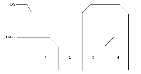
Parts 1 and 3 are controlled by the slave, the Onyx system hardware. Parts 2 and 4 are controlled by the master, and the VME controller board.
| Note: Part 1 is approximately 40 ns and Part 3 is about 20 to 25 ns. The total Onyx or POWER Onyx system contribution is about 60 to 65 ns. |
The F controller does the mapping from A32 mode into system memory and automatically crosses the page boundaries. You do not have to have AS go high and then low on 4 KB boundaries.
If you use A64 addressing, then you may have to change the address on the 4 KB boundaries and cause a transition on AS low to high, and then back to low. This incurs the delays mentioned at the beginning of this section, “Design Guidelines.”
| Note: The delays are averages and may occasionally be longer. The system design does not have any guaranteed latency. For this reason, longer transfers are better than shorter ones. If you decide to exceed the VME bus specifications, it is recommended that you place a field in a control register on your VME board that enables or disables this feature. This allows you to put the board in standard mode so it can be used on other VME systems. |
[1] Transfers of 64-bit data, accesses, and memory addresses do not depend on a 64-bit IRIX kernel, so they can be mapped to all MIPS R4000 and R8000 series platforms.