Each Origin2000 module contains three key types of ASIC: Hub, Router, and Crossbow/XIO. Within an Origin2000 system, each of these ASICs is responsible for a critical element of information transfer. The ASICs and their locations in a system are:
Hub chip: located on each Node board.
Router chip: located on each Router board in CrayLink Interconnect.
Crossbow chip: located on the midplane as part of the XIO interconnect
Bridge, LINC, and IOC3 chips: located on XIO boards linked to the I/O interface
Figure 3-1 shows interconnections between these ASICs and the communication protocols that run on the interconnections from the Hub ASIC.
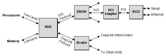
The Hub ASIC is the core of the node. It interconnects to processors, memory, CrayLink Interconnect, and the XIO interconnect.
From its processor interface, the Hub chip supports a low-level bus protocol similar to the shared-bus protocol on the CHALLENGE E-bus.
To the interconnection fabric, the Hub chip supports a high-level messaging protocol called CrayLink Interconnect, which implements the cache-coherent distributed shared-memory.
To the I/O interconnect, the Hub chip ports a separate high-level protocol called XIO, optimized for I/O devices which are not using the cache-coherence protocol.
A memory/directory protocol interfaces with the high-speed, interleaved memory system. It supports directory memory and page migration counters.
Figure 3-1 also shows Router chip and Crossbow chip interconnections. Note that the Crossbow chip uses the XIO protocol at both its input ports and output ports. Similarly, the Router chip uses the CrayLink Interconnect protocol at both its input and output ports.
Finally, the figure shows how a Bridge chip interconnects with the Crossbow and a communications controller on an XIO board; in this case, the controller is the IOC3 chip. The Bridge takes Crossbow as input, and interfaces it with the PCI protocol. The controller supported by the Bridge (the IOC3) takes PCI as input and interfaces it to Ethernet and serial.
The Origin2000 Architecture defines the theoretical model of a distributed, shared-memory multiprocessor system employing from 1 to 1024 processors.[8] Origin2000 has a single address space with cache coherence applied across the entire system.
Origin2000 is organized into a number of nodes; each node contains up to two processors, a portion of the global memory, a directory to maintain cache coherence, an interface to the I/O subsystem, an interface to the other nodes on the system, and a Hub ASIC which links all of these subsystems through a crossbar.
The Hub ASIC can be viewed as the core of the node. Physically, it is located on the Node board, and the Hub is responsible for connecting all four interfaces of the node together:
processor
memory
XIO
CrayLink Interconnect through a Router board
These are described briefly below.
Each node can have up to two R10000 processors linked to the Hub.
A portion of the distributed, shared main memory is connected to the Hub, together with directory memory used for cache coherence and page migration counts. This memory can range in size up to 4 GB.
Either one or two Hubs can be connected to each the Crossbow ASIC.
Either one or two hubs can be connected to a Router board, which in turn links the Hub to other nodes connected to the system-wide interconnection fabric.
These four interfaces are interconnected by an internal crossbar, as shown in Figure 3-2. The interfaces on the Hub communicate by sending messages through the crossbar.
The Hub controls intranode communications between the node's subsystems, and also controls internode communications with other Hub ASICs in other nodes. The Hub converts internal messages, using a request/reply format, to and from the external message format used by the XIO or CrayLink Interconnect port. All internal messages are initiated by processors and I/O devices.
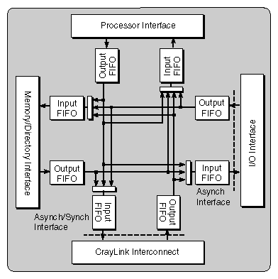
The four node interfaces act as individual controllers for their subsystems. Each interface takes inputs from an external source and converts the inputs to an internal (intra-Hub) message.
Messages can be classified as requests or replies. Each input and output FIFO associated with a Hub chip interface is logically divided into two queues; one to process requests, the other for replies. The cache coherence protocol together with the separate logical request and reply paths guarantee that deadlock is avoided.
These messages (read, write, etc.) are converted by the respective interfaces into CrayLink Interconnect requests to the appropriate target — memory or I/O interface. Depending upon the directory state, the target either replies or sends additional requests, such as an intervention or an invalidate, to other interfaces within the same or different hubs.
For example, suppose a processor sends a programmed I/O (PIO) message to a local I/O device. The message is received at the Hub chip processor interface, converted to intra-Hub format, and passed through the Hub to the I/O interface. At the I/O interface, the message is converted to XIO format and placed on the local XIO interconnect.
As shown in Figure 3-2, each Hub interface has two first-in/first-out (FIFO) buffers: one for incoming messages and one for outgoing messages. The FIFOs provide buffering between the Hub chip and the devices to which it connects. When empty, the FIFOs provide bypassing for lower latency.
The Hub ASIC provides cache coherence by:
implementing the processor portion of the Origin2000 distributed-coherence protocol
converting XIO memory requests to the Origin2000 distributed-coherence protocol
maintaining the directory caching information and migration counts for all sections of main memory
Either one or two Hubs can be connected to a Crossbow ASIC. In a dual-Hub (or dual-host) configuration, the six remaining XIO ports are statically partitioned between the two Hubs; that is, the I/O devices are assigned to one or the other of the Hubs/Node boards.
Access to an XIO device allocated to a particular hub is always made through that hub. If a remote processor accesses the device, it first communicates the request over the CrayLink Interconnect to the owning hub, which then relays the request over XIO. A statically-allocated device is local only to the Hub that owns it; to all other Hubs the I/O device is a remote device, even to a Hub physically sharing the same Crossbow ASIC.
The Router ASIC is a 6-port dynamic switch which forms the interconnection fabric connecting the nodes. Physically, the Router chip is located on a Router board, which plugs into the deskside midplane opposite the XIO and Node boards. A block diagram of the Router ASIC is given in Figure 3-3.
Functionally, the Router ASIC does the following:
Determines the most-efficient connection of receive to send ports, given the set of received messages, and dynamically switches connections between any of the six pairs of ports, through the 6-way crossbar.
Communicates reliably by using the CrayLink Interconnect link-level protocol (LLP) to other routers and hubs.
May route different messages to the same destination through different paths, for greatest speed and efficiency (adaptive routing).
To reduce latency, routes messages without having to receive the entire message (wormhole routing).
Buffers CrayLink Interconnect messages.
The block diagram shows the source-synchronous drivers (SSD) and receivers (SSR) that multiplex and demultiplex the high-speed external connection (400 MHz) to the router internal frequency (100 MHz).
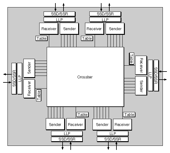
As shown earlier in Figure 2-17, three of the Router ports are STL, for rapid communication between ASICs inside the enclosure. The other three Router ports are differential PECL, for communication between modules over cables outside the enclosure. The three internal router ports use single-ended STL signalling to minimize pin count. The three external router ports use differential PECL which provides better noise immunity on external links.
The source synchronous drivers/receivers create and interpret the high speed, source synchronous signals used for communication between ASICs within the enclosure. They convert 64 bits of data transmitted at the core frequency of 100 MHz to 16 bits of data transmitted at 400 MHz.
The LLP interfaces with the SSD/SSR and provides error-free transmission of data between chips. It contains a synchronizer to interface directly with the core of the ASIC.
Error detection is made using CCITT CRC code, and correction is made by retransmission through a sliding window protocol. Both 8- and 16-bit links are supported.
The router receiver accepts data from the LLP, manages virtual channels, and forwards data to the router tables and the router sender. Dynamically Allocated Memory Queues (DAMQs) are used for efficient message handling under heavy loads. Bypass logic is provided for performance under light loads (see the section titled “Router Crossbar”). Logic also “ages” packets should they fail to make progress, giving higher priority to older packets.
The router sender drives data to the LLP for transmission to other chips. It also manages CrayLink Interconnect credits, which are used for flow control.
The routing table provides static routing information for messages as they pass through the interconnection fabric.
To minimize delays, routing table lookup is made in a pipelined fashion. Each router determines the direction the message is to take when it enters the next router. The routing table provides flexible routing and configurations with other than 2n nodes.
The router crossbar contains a series of hand-optimized multiplexers which control data flow from receiver to sender ports. Message bypassing during periods of light loading allows a message to pass through the router with minimal latency. When bypassing is not possible, a wavefront arbiter determines the optimal path.
An “aging protocol” gives priority to older messages over those more recently arrived.
The Crossbow ASIC has a dynamic crossbar switch which expands the dual-host XIO port to six 16-bit I/O ports. Each I/O port can run in either 8- or 16-bit mode, with rate-matching buffers to decouple 16-bit to 8-bit ports. At least one Crossbow port must connect and a maximum of two Crossbow ports can connect to a host. The Crossbow ASIC uses the XIO protocol at all of its ports. There are two Crossbow ASICs on each deskside midplane.
A functional view of a Crossbow ASIC, with dual hosts and six half-size XIO boards, is shown in Figure 3-4. (CrayLink Interconnect cabling is not shown in this illustration.)
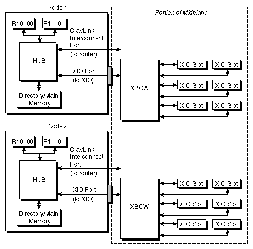
In this dual-host configuration, the six remaining XIO ports are statically partitioned between the two Node boards; if one of the host nodes is inoperable, the second host node can be programmed to take control of all the XIO ports. Note that the Node boards connect to ports 1 and 3 of the Crossbow, and the remaining six ports connect to the XIO widgets.
As described earlier, a widget is a generic term for any device connected to an XIO port. The Crossbow ASIC contains a crossbar switch that dynamically connects individual ports to particular I/O widgets (host, graphics board, serial I/O), as shown in Figure 3-5. The Crossbow decodes fields in XIO messages to determine control and destination information.
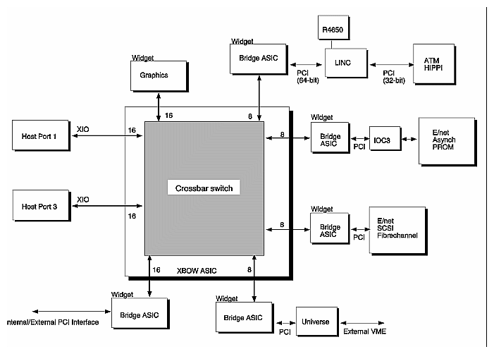
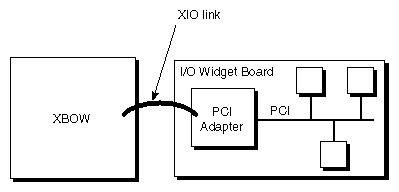
The Bridge ASIC (labelled “PCI Adapter” in Figure 3-6) is physically located on an XIO board. It converts the XIO link to the PCI bus protocol. The Bridge ASIC also provides address mapping, interrupt control, read prefetching, and write-gathering.
Peak bandwidth of the Bridge ASIC is 800 MB/sec on an XIO link and 266 MB/sec on the PCI link. There is a Bridge ASIC present on every I/O widget board.
An illustration of an I/O subsystem with a Bridge ASIC is given in Figure 3-6.
The IOC3 ASIC takes PCI output from the Bridge ASIC and converts it to standard I/O protocols for Ethernet, parallel I/O, and serial I/O. The IOC3 ASIC is physically located on the XIO BaseIO and MediaIO boards.
The LINC ASIC is designed to support intelligent controllers and optimize throughput with a variety of scatter and gather functions.
The LINC ASIC is located on the HIPPI-Serial, ATM, and OC boards; the ASIC converts the 64-bit PCI protocol to 32-bit PCI protocol. Using an IDT R4650 MIPS processor running at 132 MHz, the LINC has a 64-bit host-side “parent” PCIbus (PPCI) which provides:
64-bit addressing that is used for system DMA access
32-bit addressing that is used for peer-to-peer DMA and PIO accesses
The LINC ASIC also supports a 32-bit “child” PCIbus (CPCI) for attaching interface devices; the CPCI provides Request/Grant and interrupt support for up to two devices.
A block diagram of an I/O subsystem with both a Bridge ASIC and two LINC ASICs is given in Figure 3-7.
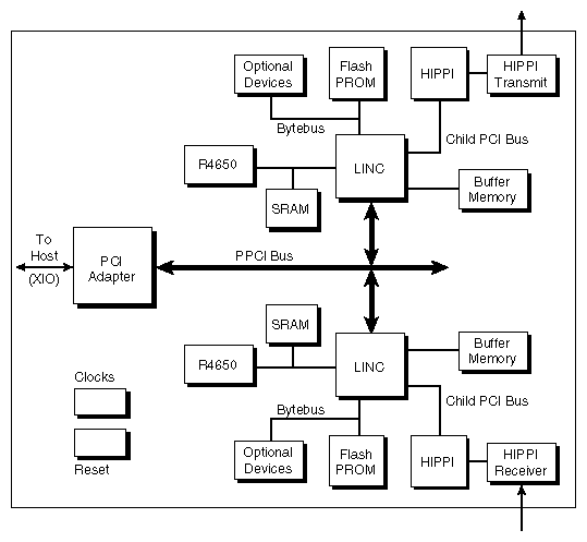
LINC ASIC also supports:
SDRAM buffer memory for local DMA
4 MB to 64 MB memory configurations, using 16 Mb or 64 Mb parts
arbitrary byte access
two DMA engines for data movement between the PPCI and buffer memory
an 8-bit bus (Bytebus) to both the Flash PROM and to slave peripherals
1-, 2-, and 4-byte access to the generic I/O device space
1-, 2-, and 4-byte reads and 1-byte writes to the Flash PROM
22 bits of address for generic devices, and 22 bits for the PROM
optional byte parity
one interrupt input
interrupt dispatch logic to the local processor, structured to minimize dispatch overhead
interrupt dispatch support to the host PCIbus
32 mailbox locations for host-to-firmware communication, with 8 bytes per mailbox located in buffer memory, and interrupt generation upon write. Mailboxes are on 64-KB boundaries for safe assignment to user code
processor Control/Status register for host management
mode pin to control autonomous boot; if inhibited, the host can release boot to PROM or to buffer memory
configuration registers for PPCI and control registers for CPCI
parity generation and checking on all ASIC boundaries (optional on the Bytebus)
support for bi-endian communication: the R4650, SDRAM, Bytebus, and all internal registers are Big Endian; byte- and word-swapping is supported on PPCI (DMA) and CPCI (DMA and PIO) per-transaction
four LED pins
four generic I/O pins