This chapter contains a description of the following boards and protocol:
Node board (Origin2000)
XIO protocol (Origin2000)
Router board (Origin2000)
Midplane board (Origin2000)
BaseIO board (Origin2000)
MediaIO board (Origin2000)
Crosstown board (Origin2000)
Motherboard (Origin200)
Daughter card (Origin 200)
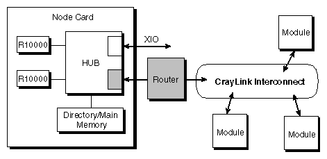
The basic building block of an Origin2000 system is the Node board, which plugs into the rear card cage of a deskside enclosure. The Node board contains the Hub ASIC with interfaces to the processor(s), memory, I/O, and CrayLink Interconnect.
Figure 2-1 shows a block diagram of the Node board, with its central Hub ASIC. The bandwidth figures represent peak bandwidth each way through the interface.
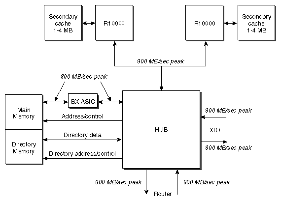
The Node board has a central Hub ASIC, to which can be connected:
either one or two processors
main memory, and its associated directory memory
the system interconnection fabric, through a dedicated Router port
I/O crossbar interconnect, through a dedicated XIO port (single port), or Crossbow ASIC (eight ports)
Bandwidths are given in Chapter 1.
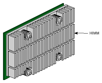
The Origin2000 system uses MIPS RISC R10000 64-bit CPU running at 195 MHz. The R10000 has separate 32-KB on-chip set associative primary instruction and data caches. Each CPU has a 1 MB or 4 MB set-associative secondary cache.
Each Node board (also referred to in this text as a “node”) is capable of supporting either one or two R10000 processors. In a deskside or rackmounted configuration, each processor is mounted on a HIMM (horizontal in-line memory module) together with its primary cache, and either 1 or 4 MB or secondary cache, as shown in Figure 2-2.
As described in Chapter 1, Origin2000 systems use distributed shared-memory (DSM). With DSM, main memory is partitioned among processors but is accessible to and shared by all of the processors. Origin2000 divides main memory into two classes: local and remote. Memory on the same node as the processor is labelled local, with all other memory in the system labelled remote. Despite this distribution, all memory remains globally addressable.
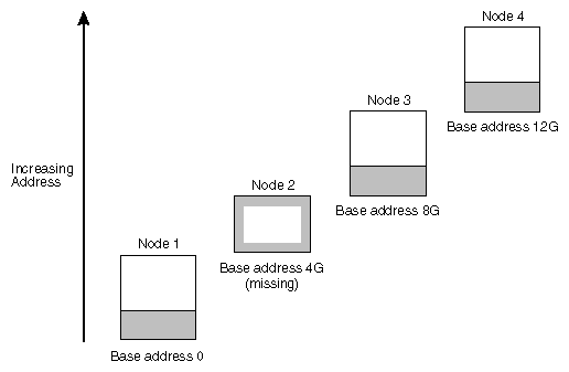
To a processor, main memory appears as a single addressable space containing many blocks, or pages. Each node is allotted a static portion of the address space—which means there is a gap if a node is removed. Figure 2-3 shows an address space in which each node is allocated 4 GB of address space, and Node 1 is removed, leaving a hole from address space 4G to 8G.
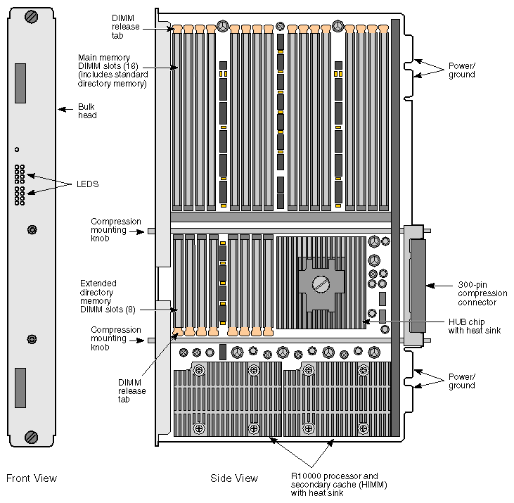
Main and directory memory are implemented using Synchronous DRAM (SDRAM) parts mounted on dual in-line memory modules (DIMMs). Each Node board has main memory that ranges in 8 increments, using pairs of DIMMs. For configurations up to 32 processors (32P), directory memory is included in the main memory DIMMs; for configurations larger than 32P, extended directory memory must be added in separate slots, as shown in Figure 2-13.
Memory DIMMs come in a range of sizes. When using 16-Mb parts, each node can support up to 1 GB of memory (in increments of 64 or 128 MB). When using 64-Mb parts, each node can support up to 4 GB of memory (in increments of 512 MB). DIMM increments can be intermixed, as long as increments are made in pairs of DIMMs.
The R10000 RISC processor uses a load/store architecture. This means data is loaded from memory into processor registers before the processor operates on the data. When the processor has finished, the data is stored back into memory. Only load and store instructions directly access main memory.
This differs from a CISC system, which can have instructions operate on data while it is still in memory. Since memory operations take longer than register operations—and there are typically several memory operations, such as calculating the addresses of the operands, reading the operands from memory, calculating and storing the result—they can negatively impact system latency.
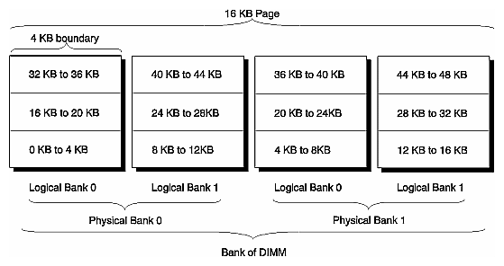
Each Node board has 16 memory slots and 8 directory slots. A memory slot holds two memory DIMMs, and the single optional directory DIMM slot is used with an extended directory. These two main memory DIMMs together with the single optional directory DIMM are referred to as a DIMM bank.
The DIMM datapath is 144 bits wide—128 bits of data and 16 bits of ECC. In a regular directory, sufficient for 32 processors, a DIMM bank also contains 16 bits of directory memory. For systems that have more than 32 processors, additional directory DIMM must be added to provide the extra 32 bits for an extended directory.
As shown in Figure 2-4, each DIMM bank has two physical banks of SDRAM, and each SDRAM has two logical banks. The four logical banks on a DIMM are interleaved at the 4 KB boundaries, and the 16K page used by Origin2000 spans all four banks on the DIMM.
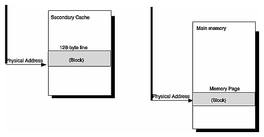
The smallest unit of data that can either be present or not present in memory is broadly referred to as a block; a block is also the smallest unit of data over which coherence is maintained.
More specifically, a block of data in a cache is called a line, as in “cache line.” In Origin2000, secondary cache lines are fixed in size at 32 words, or 128 bytes. A block of data in main memory can have a different name: a page, as in a “page in memory.” Main memory page sizes are multiples of 4 KB, usually 16 KB.
| Note: In main memory, coherence is maintained over a cache line, not a page. |
Depending on the cache,[2] lines are accessed, or indexed, using either a virtual or a physical address. Pages in main memory are indexed with a physical address. This process is shown in Figure 2-5.
Virtual memory, or virtual addressing, is used to divide the system's relatively small amount of physical memory among the potentially larger amount of logical processes in a program. For instance, let's say a system has 32 MB of main memory, and it is being used by 10 users, each of whom have 100 processes. Dividing physical memory equally would limit each user process to a minuscule 32 KB of memory. Alternatively, it would be too expensive to dedicate a full 32-MB address space to each process: this would require 32 GB of physical memory.
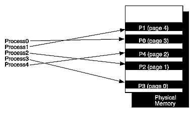
Instead, virtual addressing provides each process with a “virtual” 32 MB of memory, as shown in Figure 2-6. It does this by dividing physical memory into pages, and then allocating pages to processes as the pages are needed. In an action called mapping, each physical page links or “maps” its physical address to the virtual address of the process using it.
These virtual-to-physical address mappings can be found in several places:
a software table in main memory called a page table; each entry in the table is called a page table entry, or PTE
several R10000 processor registers used for memory management, if the page has been recently retrieved
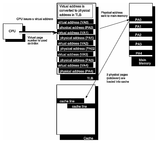
a hardware buffer called a translation lookaside buffer, which acts as a cache for quick retrieval of recently-used virtual-to-physical address mappings
References to the page table in main memory can be time consuming. To reduce this latency, a subset of the page table is stored in a fast buffer of registers called a translation lookaside buffer. The TLB allows rapid access to the most-recently-used address translations.
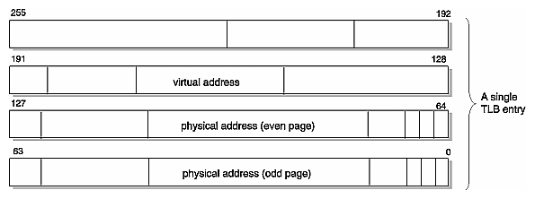
Figure 2-8 shows a part of a virtual-to-physical address mapping, as it is contained in the R10000 TLB. Each entry is 256 bits (8 words) long. Notice that each virtual address maps to a pair of physical pages: an even-numbered page (for instance, page 0) and its corresponding odd-numbered page (page 1).
When a process finds a cache line it is looking for, it is said to make a hit in the cache. However, sooner or later a process fails to find the line it is looking for in the cache. This is called a cache miss. When the process can't find a page in main memory, this failure is called a fault, as in “page fault.”
In a cache miss or a page fault, the next lower level(s) of memory hierarchy are searched for the missing data.
Simply put, coherence is the ability to keep data consistent throughout a system. Data coherence in a uniprocessor system is usually managed directly by the processor, so no separate coherence protocol is needed.
A multiprocessor configuration is different. In a system like Origin2000, data can be copied and shared amongst all the processors and their caches. Moving data into a cache reduces memory latency, but it can also complicate coherence since the cached copy may become inconsistent with the same data stored elsewhere. A cache coherence protocol is designed to keep data consistent and to disperse the most-recent version of data to wherever it is being used.
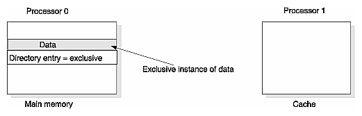
Here's an example of cache coherence. It starts when a new block of data is loaded into a single processor's cache. Since there is only one instance of this data in the entire system, the coherence state of the data is said to be Exclusive, as shown in Figure 2-9. This state is indicated by setting the Exclusive bit in the directory entry that is assigned to the memory block (see “Directory-Based Coherence” for a description of directory-based coherence).
When Processor 1 needs to use this data, it makes a copy and loads the copy into its cache. This means there are now two instances of the same data in the system, which also means the data in Processor 0 is no longer exclusive.
When the copy is made, the directory sets the Shared state bit, indicating that this block has a copy somewhere[3] in the system. This is shown in Figure 2-10.
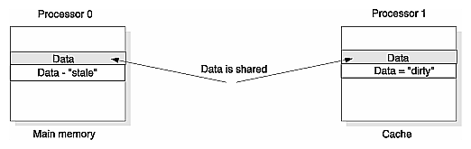
Processor 1 uses the data. If the data has been changed, it is referred to as dirty and is marked for writeback.[4]
Once Processor 1 is finished using the data, the next step is for Processor 1 to write this data into its cache. However, if this write were allowed to execute there would be two different versions of the same data in the system: the newly-modified data in Processor 1 cache, and the unmodified, or “stale” version in the main memory and cache of Processor 0. Therefore the stale data must be made consistent with the dirty version in Processor 1 cache.
There are two different methods, called protocols, of reconciling the inconsistency between the versions of data:
snoopy-based protocol (see the section titled “Snoopy-Based Coherence”).
directory-based protocol (see the section titled “Directory-Based Coherence”).
Origin2000 uses a directory-based coherence protocol.
Challenge is an example of a snoopy-based system. All processors are connected to a single, shared bus. Each processor is responsible for monitoring, or “snooping,” this bus for memory reads that might affect the data in its cache—for instance, a write to shared data, or a read of clean data. Each processor is also responsible for broadcasting each of its cache misses to the entire system.
Snoopy protocols are generally used on small-sized systems; given the speed of today's RISC processors, requiring all cache misses to be broadcast can quickly swamp a bus. Obviously this would also limit the growth, or scalability, of the system, since adding more processors to the bus would only serve to saturate it more quickly.
Origin2000 uses a directory-based coherence protocol. In a directory-based protocol, each block in memory has an accompanying directory entry. These entries are kept in a table called a directory. Since memory is distributed throughout the system, directories and their entries are also distributed.
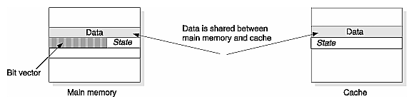
As shown in Figure 2-11, each directory entry contains information about the memory block such as its system-wide caching state, and bit-vector pointing to caches which have copies of the memory block. By checking the state and the bit vector, memory can determine which caches need to be involved with a given memory operation in order to maintain coherence.
Directory-based coherence avoids the bandwidth problem of a snoopy protocol by not requiring each processor to broadcast their memory accesses. Instead, only those caches which contain copies of the memory block need to be notified of a memory access, and then only if they are affected. This feature of the directory protocol assures that the scalable bandwidth of the interconnection fabric is not compromised by the support of cache coherence.
Two methods may be used to maintain coherence in a directory-based system: update, and invalidate. Origin2000 uses the invalidate method.
An invalidate purges all copies of the modified, or dirty, cache line from all other caches in which the line resides. Invalidation is done by setting an Invalid bit in the cache line's tag. If an invalidate is executed, the single remaining line becomes exclusively owned by the writing processor. Invalidation allows the processor having exclusive ownership to make further writes to the line without having to notify other caches as each write occurs.
Were cache coherence not implemented in hardware, the responsibility for coherence would fall either to the user or to the compiler. Neither of these alternatives are preferable, since:
leaving its responsibility to the user could greatly complicate the programming effort, and
leaving its responsibility to the compiler greatly complicates the compiling effort and forces the compiler to conservatively limit the amount of caching.
Designing coherence into the hardware allows the compiler to concentrate on optimizing for latencies.
Various models are used to maintain data coherence throughout a computer system. The most stringent model is called sequential consistency, which is used in Origin2000.
Using sequential consistency,
all processors issue memory requests in program order
all memory operations return values that correspond to a sequential ordering of the memory references by the processors.
Ordering is enforced between uncached writes and cached operations, but overlap is still possible due to the design of the R10000.
Origin2000 uses four stable states and three transient states for the directory.
Unowned: (uncached) the memory block is not cached anywhere in the system
Exclusive: only one readable/writable copy exists in the system
Shared: zero or more read-only copies of the memory block may exist in the system. Bit vector points to any cached location(s) of the memory block.
Busy states: Busy Shared, Busy Exclusive, Wait. These three transient states handle situations in which multiple requests are pending for a given memory location.
Poisoned: page has been migrated to another node. Any access to the directory entry causes a bus error, indicating the virtual-to-physical address translation in the TLB must be updated.
| Note: Directory poisoning is an architectural feature which is being proposed for future implementations. In implementations where directory poisoning is unavailable, the operating system uses a more conventional TLB shootdown algorithm to handle the TLB updates required by page migration. |
A read cycle traversing the memory hierarchy is described below.
The processor issues a read request to its cache.
If data is present, the processor continues execution.
If data is not present—a cache miss—the read request is passed on to the home node of the memory (home may be either local or remote).
The read request is made to home memory. If block is in home memory, fetch it. Simultaneously, check the coherence state of the block's directory entry.
If data is Unowned, return data to requestor and update directory entry to Exclusive.
If data is Shared, return the data to requestor and update the directory to Shared, and set the appropriate bit in the vector for the requesting processor.
If data is Exclusive, pass the read request from home memory to the remote memory that owns the Exclusive copy. Go to the next level of hierarchy.
Remote memory returns the Exclusive copy of data directly to the requesting processor. In parallel with this operation, a sharing write back is executed to home memory, updating the directory entry to indicate the fact that both the remote memory and the requesting processor are now sharing this block.
Making the two operations in Step 3 parallel reduces the latency of a remote-memory read request.
A write cycle traversing the memory hierarchy is described below.
The processor issues a write request to its cache.
If data is present in the cache—a cache hit—and the data is in a Clean Exclusive or Dirty state, the write can complete immediately and processor execution continue.
If data is present but not Clean Exclusive or Dirty, a processor upgrade request is issued to the home memory to obtain exclusive ownership of the data. This home memory can be either local or remote.
If data is not present—a cache miss—a read-exclusive request is issued to home memory.
The read-exclusive or upgrade request is passed to home memory. Home memory can service an ownership request for a memory write of a location that is either Unowned or Shared.
If the write is to a home memory block that is in the Shared state, all other copies of the block must be invalidated. The home memory directory has a bit vector which points to any node(s) holding a copy of this block, and invalidations are sent to each of these nodes. The home replies to the write requester of Step 1 by sending either an Exclusive data reply in the event of a Read-Exclusive request,[5] or an Upgrade acknowledgment in response to an Upgrade request.
If the write is to a home memory block that is in the Exclusive state, the read-exclusive request is sent on to the node that owns the Exclusive data.
Result of a read-exclusive request ripples out to remote memory in the following cases:
If the write request is to a Shared memory block, remote nodes receive Invalidate requests to eliminate their Shared copies. As each cache line is invalidated, the node sends an Invalidate Acknowledge back to the write requestor.
If the write request is to a Exclusive memory block, the remote owner of the Exclusive data receives a read-exclusive request. The remote node then takes the following two actions:
It returns the requested data directly to the write requestor.
It sends a transfer message to the home directory indicating that the write requestor now owns Exclusive data.
Memory latency is the amount of time it takes a system to complete a read or write to memory. It is quoted using two metrics: access time and cycle time.
Memory latency is reduced by:
the inherent spatial and temporal locality in caches
distributing memory, and moving some of it close to each processor
page migration, in which frequently-accessed data is moved from remote memory to local memory
the integrated node design and CrayLink Interconnect topology, which reduces the number of chip crossbars and the contention to reach remote memory.
Locality and page migration are describing in the sections below; memory distribution is described in Chapter 1.
Cache memory is designed to take advantage of a fundamental property of programming: a program usually spends 90% of its execution time running 10% of its code. This is a result of what is called locality of reference: programs tend to reuse data and instructions they recently used.
Programs exhibit two types of locality:
temporal: items that have been recently accessed are likely to be accessed again in the near future
spatial: a program tends to reference items whose addresses are close to each other
Caches are designed to exploit this principle of locality by storing small subsets of main memory for rapid accessibility. Using the two principles of locality described above, a cache contains the most-frequently-used information needed by the processor.
To provide better performance by reducing the amount of remote memory traffic, Origin2000 uses a process called page migration and replication. Read-only pages are replicated; read/write pages are migrated. Page migration and replication moves data that is often used by a processor into memory close to that processor. Data is moved by a specially-designed Block Transfer Engine, (BTE).
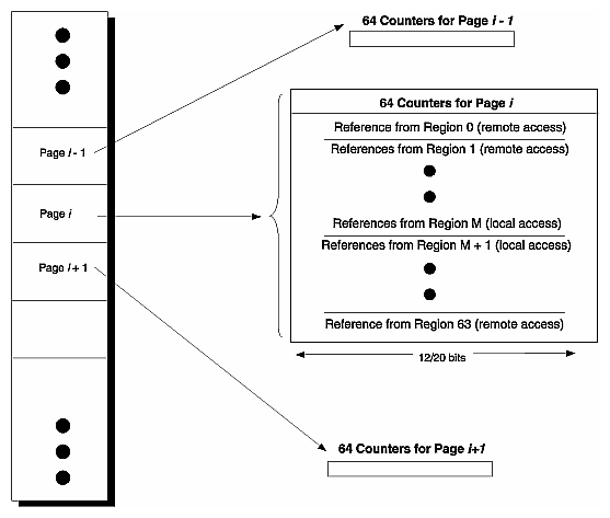
Each page has an array of 64 page-reference counters—one counter for each node. These counters track the number of memory references to a line by a given node. During a memory operation, the counter for the requestor is compared against the counter for the home node—Remote Access and Local Access counters, respectively—to determine which pages should be migrated closer to the using processors. When the difference between the Access counters exceeds a certain software-determined threshold, the hardware generates an interrupt to the operating system (OS), indicating an excess number of accesses has been made to the remote page. The OS then to an interrupt handler.
Once in the interrupt handler, the OS uses a migration algorithm to decide whether or not to migrate/replicate the page. If the decision is made to replicate or migrate the page, the page is moved to a physical page on the node that is issuing the remote access. This action is taken while the OS is still in the interrupt handler.
| Note: After the page has been moved, its TLB entry must be updated. In implementations where directory poisoning is unavailable, the operating system uses a more conventional TLB shootdown algorithm to handle the TLB updates required by page migration. |
As shown in Figure 2-12, the per-page Local Access and Remote Access counters keep their counts on a regional basis. When there are less than 128 CPUs in a system, a region is defined as two processors sharing a hub. When a system is larger than this, a region is defined as eight hubs in the same node. The present Origin2000 system has 64 regions, one for each two-processor node.
The Access counters can have two widths, depending upon whether regular or extended directory DIMMs are used. The counter width is 12 bits with regular DIMMs and 20 bits with extended DIMMs.
| Note: Directory poisoning is an architectural feature which is being proposed for future implementations. In implementations where directory poisoning is unavailable, the operating system uses a more conventional TLB shootdown algorithm to handle the TLB updates required by page migration. |
After the page has been moved, TLBs must be updated to point to the new location of the page. Since transmitting updated address mappings to all TLBs could be quite slow, the source page (the page being copied) is instead “poisoned” during the copy operation, by setting the Poisoned state bit in the page's directory entry.
Once the Poisoned bit is set, any access to the old TLB entry returns a special bus error to update the TLB. The interrupt handler for this bus error still has the virtual address the CPU was attempting to access, and now uses this virtual address to invalidate, or “shoot down” the TLB entry.[6] The next time the CPU accesses this TLB entry, either an updated or an invalid translation is returned. If an invalid translation is returned, this page is migrated and then the newly-updated translation is loaded into the TLB.
Poisoning the block's directory entry allows global migration of pages without the overhead of having to do a global TLB invalidation of all the relevant TLB entries.
All processors can also access any I/O port as a location in uncached memory address space. Likewise, DMA access is provided for all DMA devices to all memory in the system.
One Hub can be designated a clock “master,” sending a global clock out through the routers to the rest of the Hubs, which then slave off this clock. An optional BNC connector on the edge of the Node board can feed an external 1 MHz TTL real-time clock to the system, if greater accuracy is needed.
Nodes are linked by the interconnection fabric, through a Router card. Node boards can be installed in either graphics or server modules. Each Node board connects to the module midplane through a 300-pin connector.
A physical view of the Node board is given in Figure 2-13.
Origin2000 systems use an advanced input-output (I/O) subsystem, consisting of a number of high-speed XIO links. XIO supports a wide range of Silicon Graphics and third-party I/O devices.
XIO bandwidth is given in Chapter 1 of this document.
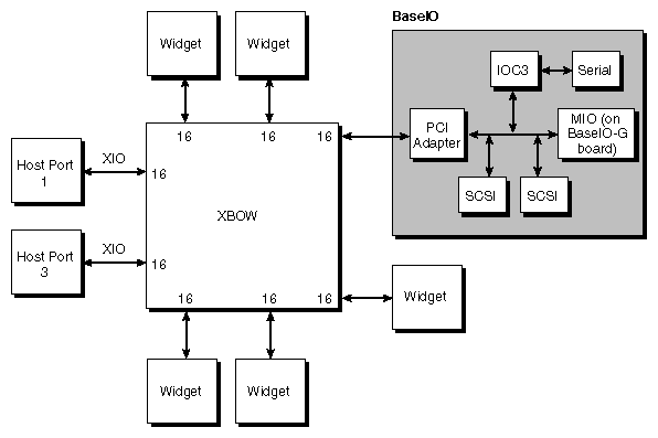
XIO is distributed, with an I/O port on each Node board. As with Origin2000 distributed memory, each I/O port is accessible by every CPU. I/O is controlled either through the single-port XIO-protocol link on the Node board, or through an intelligent crossbar interconnect on the Crossbow ASIC.
A Crossbow ASIC expands the single XIO port to a total of eight ports: six are used for I/O and two connected to Node boards. Ports using the XIO protocol can be programmed for either 8 or 16 bits communications. The electrical interface for XIO is the same as that used by CrayLink Interconnect.
The form-factor for XIO widgets[7] may vary. Typically a widget is a single board, either half-size (10-inch x 6.5-inch x 1-inch) or full-size (10-inch x 13-inch x 1-inch); however it is possible for a widget to include a daughter board.
XIO can also run outside an enclosure, using the Crosstown protocol, which is described in the section titled “Crosstown Board.”
An example of a Crossbow (XBOW) configuration, with 4 CPUs (2 Node boards) and 6 I/O ports, is given in Figure 2-14. In this example the Crossbow is presented in a graphics configuration, connected to two graphics boards as well as four XIO boards.
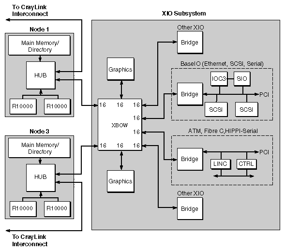
A number of interface ASICs are available to link the Crossbow ports to PCI, VME, SCSI, Ethernet, ATM, FibreChannel, and other I/O devices. The interface ASICs include the IOC3, LINC, and Bridge ASICs, all of which are described in Chapter 3.
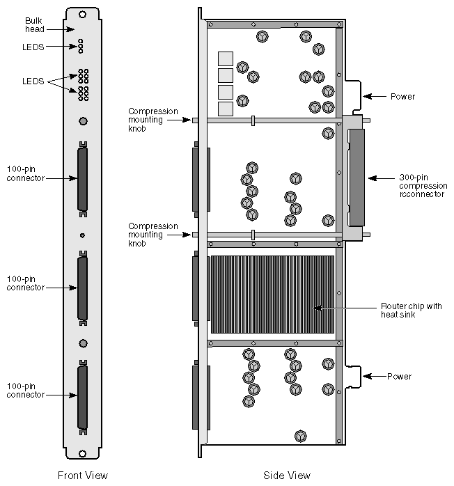
Router boards physically link the Hub ASIC on the Node board to the CrayLink Interconnect. The CrayLink Interconnect provides a high bandwidth, low latency connection between all the Node boards. Central on a Router board is the Router ASIC which implements a full 6-way non-blocking crossbar switch.
Location of a Router board in a system is shown in Figure 2-15, and a physical view of the Router board is given in Figure 2-16.
The Router crossbar allows all six of the Router ports to operate simultaneously at full-duplex; each port consists of two unidirectional data paths. The Router board also includes a set of protocols which provides a reliable exchange of data even in the face of transient errors on links, manages flow-control, and prioritizes data so that older data is given precedence over newer data.
Bandwidth figures are given in Chapter 1 of this document.
There are four types of Router boards:
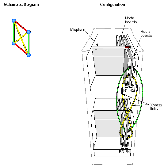
The Null Router connects two Node boards in the same deskside enclosure (up to four R10000 processors). The Null router configuration cannot be expanded.
The Star Router connects up to four Node boards to each other. 3- and 4-Node configurations are created using a Standard router with a Star router.
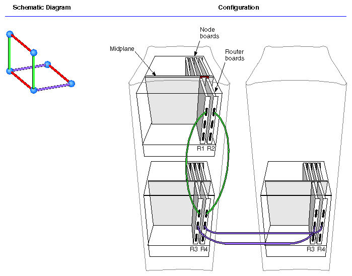
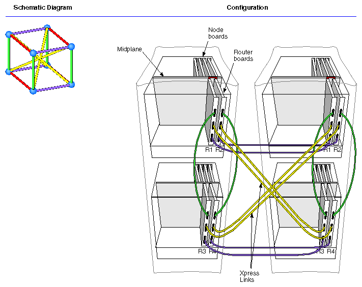
The Standard Router cables together from 2 to 32 Node boards (from 2 to 64 CPUs), physically located in from 1 to 8 enclosures.
The Meta Router is used in conjunction with Standard routers to expand the system from 33 to 64 Node boards (65 to 128 CPUs) in a hierarchical hypercube that will be available sometime in the future.
Programmable tables within the Router ASICs control packet routing through the CrayLink Interconnect. These tables allow for partial configurations (system sizes which are not 2n) and reconfigure around broken links or inoperative modules.
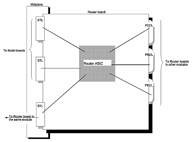
Each port on the Router board consists of a pair of 16-bit unidirectional links that provide 800 MB/sec of peak bandwidth each way (1.6 GB/sec bidirectional). The links use a Silicon Graphics-developed low-swing CMOS signalling technology (STL).
STL provides direct, very high-speed (2.5 ns cycle time) ASIC-to-ASIC communication inside an enclosure. These STL links can be buffered with differential ECL transmitters and receivers to drive cables to run outside the enclosure, connecting to other modules.
| Note: Proper operation of the external modules requires correct grounding of the attached modules. Proper site preparation is essential for reliable operation. |
As shown in Figure 2-17, a Standard Router board has six CrayLink interconnections; three are used for STL midplane links, three are used for external PECL cable links.
The three midplane connections are built into 300-pin connectors. The three cable connectors are on the board bulkhead. Two of the STL connectors support links to Node boards, and the third supports a link to a second Router board in the module (if present). Each of the external connectors supports a cable connection to another Router board, either in the same module or in another module.
Additional CrayLink interconnections, called Xpress links, can be installed between Standard Router ports for increased performance (reduced latency and increased bandwidth).
Xpress links can only be used in systems that have either 16 or 32 processors. Each Xpress link provides additional bandwidth of 800 MB/second each way (1.6 GB bidirectionally, peak).
Figure 2-18, Figure 2-19 and Figure 2-20 illustrate 16-, 24- and 32-processor systems, respectively.
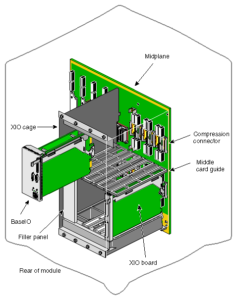
The Origin2000 Midplane board is a backplane that has been moved to the center of the deskside enclosure. Figure 2-21 shows the physical location of the midplane in relation to the deskside chassis. Also shown is the Node board placement in the midplane.
Functionally, the midplane provides the following:
a standard system clock for both the XIO and CrayLink interconnection
STL links for the CrayLink Interconnect and XIO links within the module
power distribution throughout the system
system control signals and additional real-time clock distribution
digital media sync
SCSI connections
Physically, the components located on the midplane are:
four 300-pin STL connectors for four Node boards
two 300-pin connectors for two Router boards
twelve 96-pin connectors for twelve half-size XIO boards
five connectors for five wide, single-ended Ultra-SCSI disk drives
one connection for a 680 MB quad-speed CDROM
one connection for a System Controller
two SysClocks:
400 MHz CrayLink Interconnect clock for Hub and Router ASICs
400 MHz I/O clock for Hub, Crossbow, and Bridge ASICs
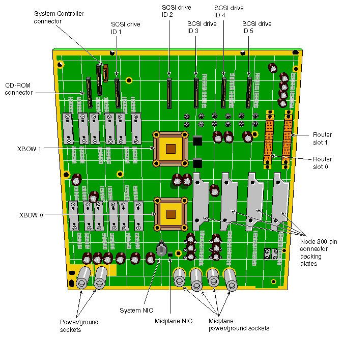
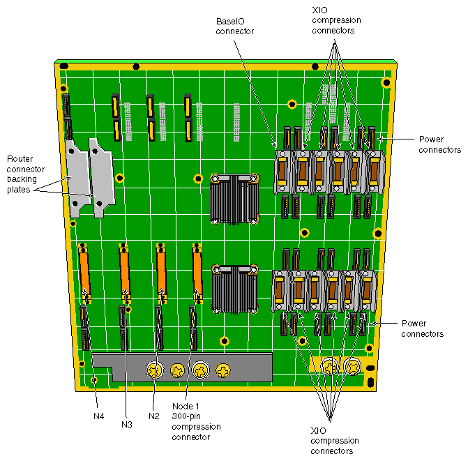
A a front view of the Origin2000 midplane is shown in Figure 2-22, and a rear view of the midplane board is shown in Figure 2-23.
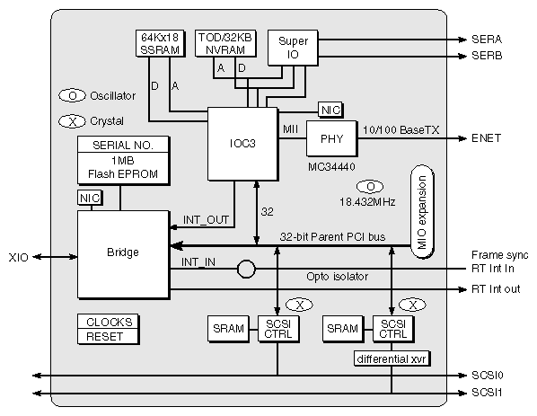
The BaseIO board contains those I/O functions which come standard in each base system enclosure:
one 10/100 Base TX Fast Ethernet link, with auto-negotiation (compliant with 802.3u)
two 460-Kbaud serial ports, composed of dual, independent UARTS
one external, single-ended, wide SCSI (compliant with X3.131-1994) port
one internal Fast 20 SCSI (compliant with X3.131-1994) port
one real-time interrupt output, for frame sync
one interrupt input
Flash PROM
NVRAM
Time-of-Day clock
The logical location of a BaseIO card, connected to a Crossbow ASIC, is illustrated in Figure 2-24. The block diagram of the BaseIO board is shown in Figure 2-25.
Due to the size of the BaseIO board, only one can be installed in each deskside enclosure. In a multi-enclosure system, there can be as few as one BaseIO board for the entire system, or there may be a BaseIO board installed in each deskside enclosure. Enclosures which do not have a BaseIO board installed can install other XIO cards in midplane BaseIO slot.
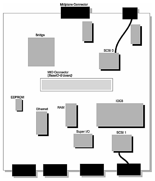
The physical layout of the BaseIO board is shown in Figure 2-26.
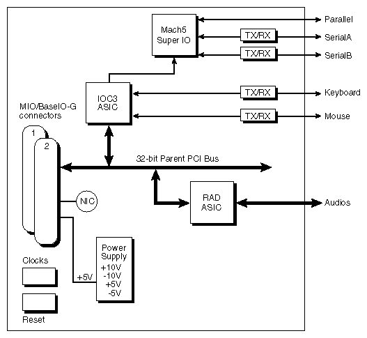
A Media IO (MIO) daughter card can be plugged into a modified BaseIO board, called the BaseIO-G board. The MIO card is plugged into the BaseIO-G board's PCI bus to provide additional audio and serial ports.
The Media IO board (MIO) is mounted as a daughterboard on a specially-configured BaseIO board, called the BaseIO-G board. The MIO is primarily used in graphics systems to provide additional audio, serial, keyboard/mouse, and parallel ports. Specifically, the MIO board adds the following to an BaseIO-G board:
one IEEE 1284 parallel port
two 460-Kbaud serial ports, dual independent UARTS
one audio analog stereo input port
one audio analog stereo output port
one audio AES3/AES11/SPDIF digital input port
one audio AES3/AES11/SPDIF digital output port
one audio Alesis ADAT/Optical SPDIF digital fiber input port
one audio Alesis ADAT/Optical SPDIF digital fiber output port
one keyboard port
one mouse port
The majority of audio functions are provided by the RAD ASIC.
Dues to its size, there can only be one BaseIO/BaseIO-G board per deskside enclosure. Since an MIO board is mounted as a daughterboard on the BaseIO-G board, there can also only be one MIO board in a deskside enclosure. If more than one MIO is desired, it must be added to a multi-enclosure system in which additional BaseIO-G boards can been installed as well.
The BaseIO-G and MIO are treated as an atomic module when MIO functions are used.
The logical location of an MIO card, connected to an BaseIO-G board, is shown in Figure 2-24. A block diagram of the MIO board is shown in Figure 2-27.
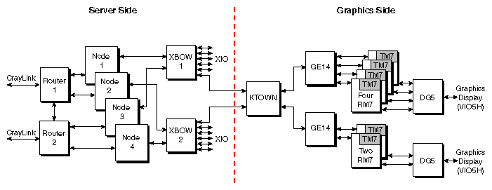
XIO can also run outside an enclosure, using the Crosstown (KTOWN) conversion board. For example, an XIO slot may be occupied by a Crosstown board, which contains an STL-to-3.45V PECL converter and a Crosstown cable attachment; the result is to convert the XIO STL link to differential signal levels. This connection can support XIO devices up to 3 meters away. Crosstown is primarily used to support graphics configurations.
A block diagram of an Origin2000 system using a Crosstown link is shown in Figure 2-28.
An illustration of the Origin200 mother and daughter boards is given in Chapter 1. Each mother board can hold 1 to 2 R10000 processors each with 1 or 4 MB of secondary cache. The processors and cache memory are located on a separate daughterboard which mounts to the motherboard.
The motherboard can hold from 32 MB to 2 GB of main memory.
[2] Primary caches are indexed with a virtual address, while the secondary cache is indexed with a physical address. Physical and virtual addressing are described in the section, “Virtual Memory.”
[3] That “somewhere” is indicated by a bit vector in the same directory entry, which points to the node(s) storing the shared copy.
[4] This applies to read/write data only. Since read-only data cannot be modified, it does not need to be written back.
[5] At this time the home also changes its own state to Exclusive.
[6] This is also known as a “lazy” TLB shootdown.
[7] I/O devices are pseudonymously referred to as “widgets.”